System for reducing peak power during scan shift at the global level for scan based tests

a global level and scan based test technology, applied in the field of integrated circuit testing, can solve the problem of reducing the overall test time during a production test, and achieve the effect of reducing peak power problems, high, and reducing peak power issues

Active Publication Date: 2014-07-03
NVIDIA CORP
View PDF7 Cites 10 Cited by
  • Summary
  • Abstract
  • Description
  • Claims
  • Application Information

AI Technical Summary

Benefits of technology

[0009]Accordingly, a need exists for a system that allows scan shift operations to run fast at high clock speeds while reducing peak power issues caused by the high toggling rate and logic activity during scan shift mode during DFT. It is also necessary to make the scan test mode power-aware to avoid stressing the power distribution network in test mode during production testing. Embodiments of the present invention provide a method and system for reducing peak power problems during scan shift mode at the global level.

Problems solved by technology

This allows the scan shift operations to be run at higher clock speeds, which in turn eventually reduces the overall test time during a production test.

Method used


Image

  • System for reducing peak power during scan shift at the global level for scan based tests
  • System for reducing peak power during scan shift at the global level for scan based tests
  • System for reducing peak power during scan shift at the global level for scan based tests

Examples


Embodiment Construction

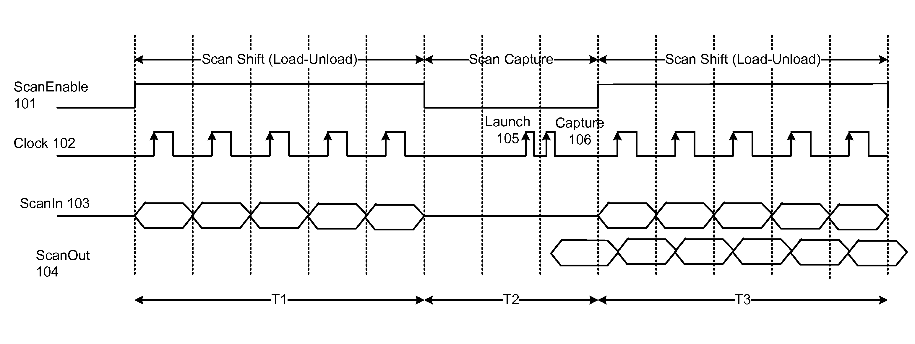
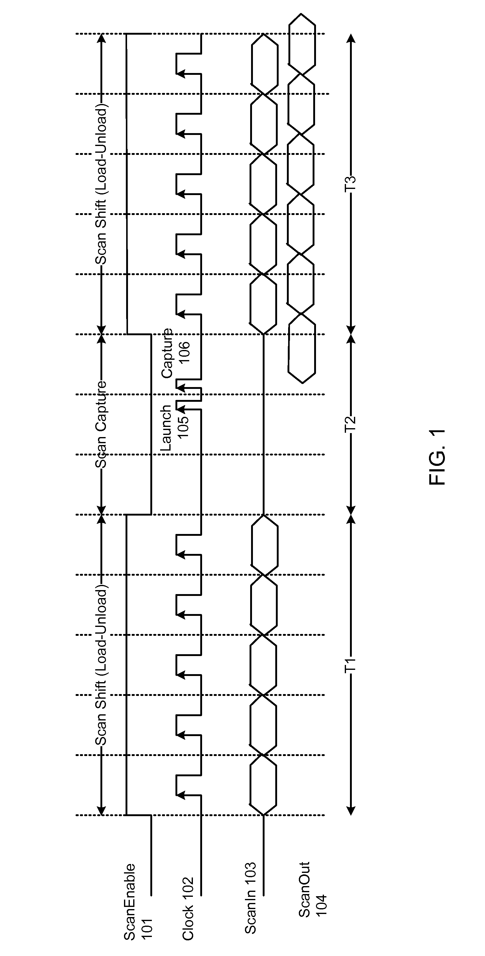
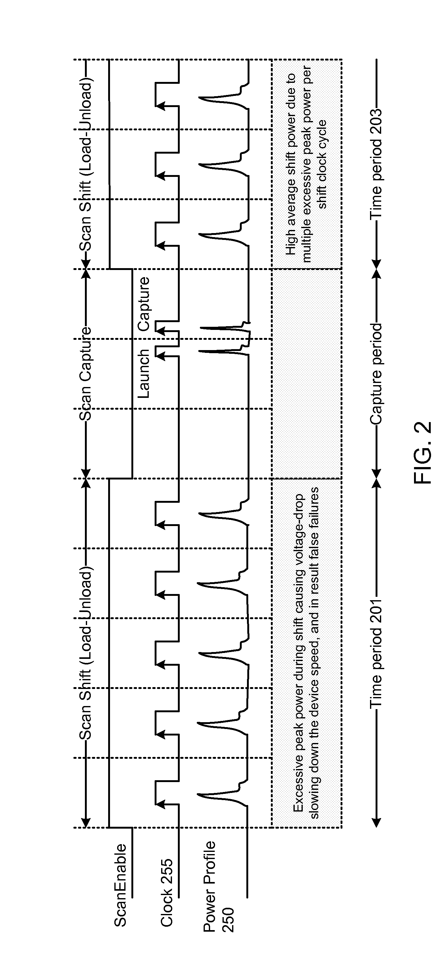
[0033]Reference will now be made in detail to the various embodiments of the present disclosure, examples of which are illustrated in the accompanying drawings. While described in conjunction with these embodiments, it will be understood that they are not intended to limit the disclosure to these embodiments. On the contrary, the disclosure is intended to cover alternatives, modifications and equivalents, which may be included within the spirit and scope of the disclosure as defined by the appended claims. Furthermore, in the following detailed description of the present disclosure, numerous specific details are set forth in order to provide a thorough understanding of the present disclosure. However, it will be understood that the present disclosure may be practiced without these specific details. In other instances, well-known methods, procedures, components, and circuits have not been described in detail so as not to unnecessarily obscure aspects of the present disclosure.

[0034]S...


PUM


Abstract

A method for reducing peak power during a scan shift cycle is presented. The method comprises multiplexing a test clock with a functional clock on a integrated circuit at the root of a clock tree. The method also comprises adding a plurality of delay elements on a clock path, wherein the clock path is a signal resulting from the multiplexing. Further, the method comprises routing the clock path to a plurality of cores and a cache, e.g., an L2C cache, on the integrated circuit. Finally the method comprises staggering the test clock received by each of the plurality of cores and the cache by employing the delay elements during a scan shift cycle.

Description

CROSS-REFERENCE TO RELATED APPLICATIONSRelated Applications[0001]The present application is a continuation-in-part of U.S. patent application Ser. No. ______, filed ______, entitled “SYSTEM FOR REDUCING PEAK POWER DURING SCAN SHIFT AT THE LOCAL LEVEL FOR SCAN BASED TESTS,” naming Milind Sonawane, Satya Puvvada and Amit Sanghani as inventors, and having attorney docket number NVID-PSC-11-0240-US1. That application is incorporated herein by reference in its entirety and for all purposes.FIELD OF THE INVENTION[0002]Embodiments according to the present invention generally relate to testing integrated circuits and more specifically to performing scan based tests on integrated circuits.BACKGROUND OF THE INVENTION[0003]An integrated circuit or circuit assembly generally contains one or more clocks, either generated internally or controlled externally. Each clock is distributed to a set of storage cells via a skew-minimized network, which delivers a clock pulse to all the storage cells at v...

Claims


Application Information

Patent Timeline
Patent Type & Authority Applications(United States)
IPC IPC(8): G01R31/3177
CPCG01R31/3177G01R31/318552G01R31/318575
Inventor SONAWANE, MILINDPUVVADA, SATYASANGHANI, AMIT
Owner NVIDIA CORP
Why Eureka
Try Eureka