CMOS transistors, fin field-effect transistors and fabrication methods thereof
- Summary
- Abstract
- Description
- Claims
- Application Information
AI Technical Summary
Benefits of technology
Problems solved by technology
Method used
Image

Examples
Embodiment Construction
[0016]Reference will now be made in detail to exemplary embodiments of the invention, which are illustrated in the accompanying drawings. Wherever possible, the same reference numbers will be used throughout the drawings to refer to the same or like parts.
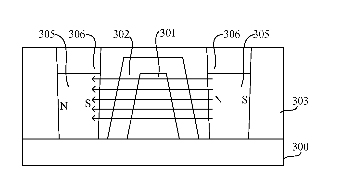
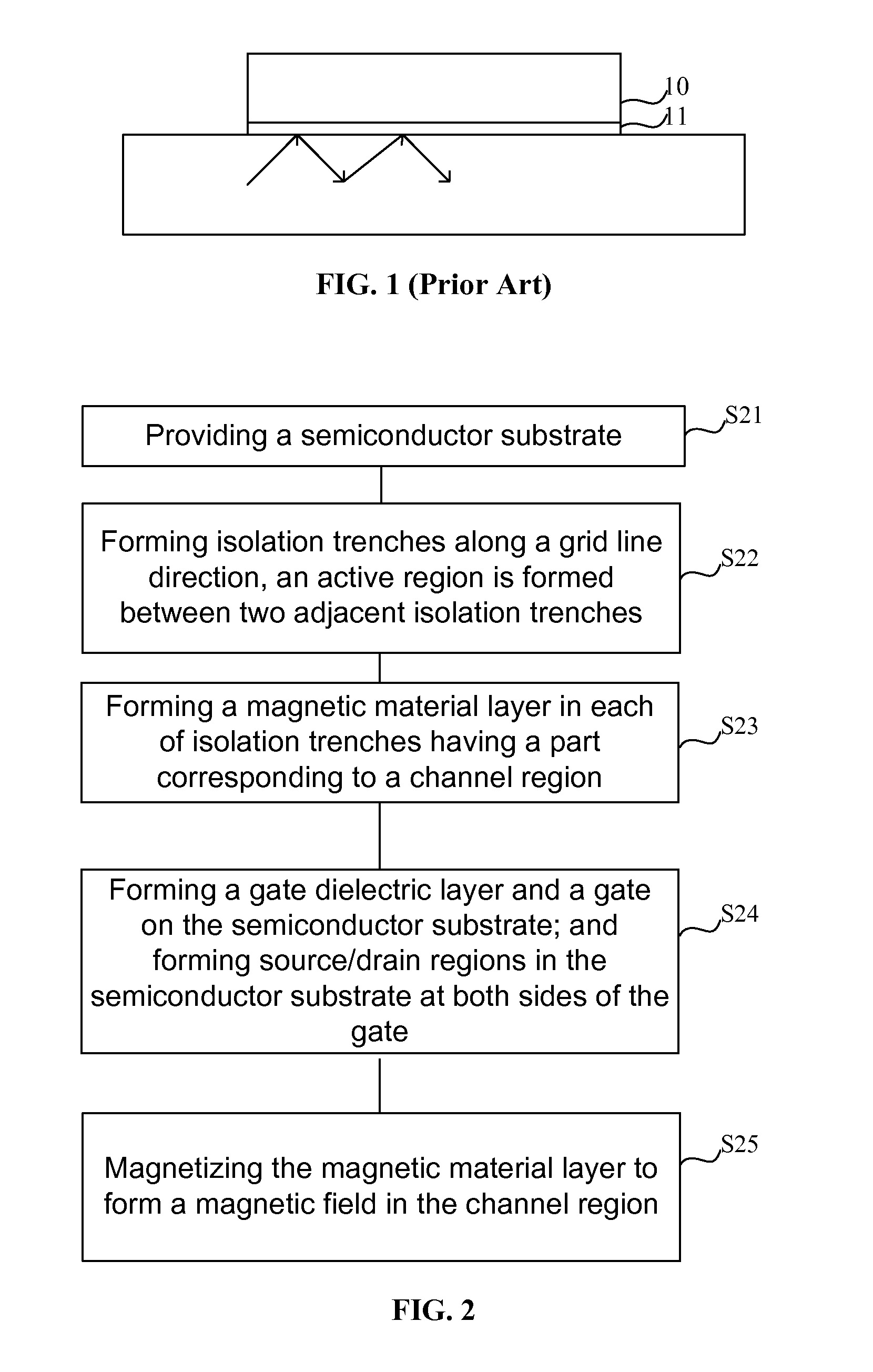
[0017]FIG. 2 illustrates an exemplary fabrication process for a CMOS transistor consistent with the disclosed embodiments, and FIGS. 3-12 illustrate exemplary semiconductor structures corresponding to various stages of the fabrication process.
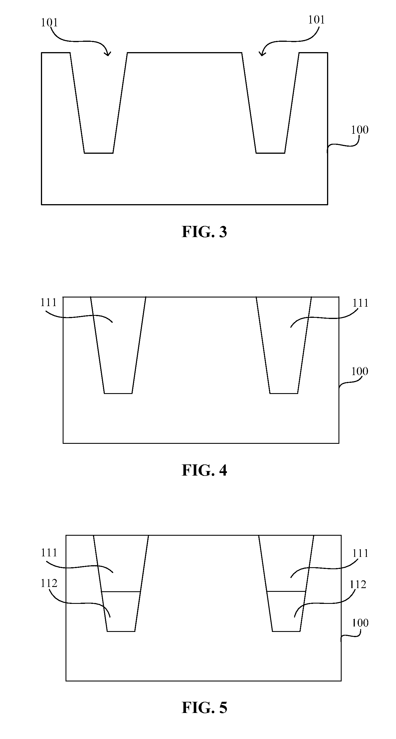
[0018]As shown in FIG. 2, at the beginning of the fabrication process, a semiconductor substrate with certain structures is provided (S21). FIG. 3 illustrates a corresponding semiconductor structure.
[0019]As shown in FIG. 3, a semiconductor substrate 100 is provided. The semiconductor substrate 100 has a plurality of insulation trenches 101 in one surface.
[0020]The semiconductor substrate 100 may include any appropriate semiconductor material, such as silicon, silicon on insulator (SOI), silic...
PUM
 Abstract
Description
Claims
Application Information