Finfet integrated circuits with uniform fin height and methods for fabricating the same

a technology of integrated circuits and fins, which is applied in the direction of semiconductor devices, electrical apparatus, transistors, etc., can solve the problems of reducing the distance between the source region and the drain region, affecting the electrical potential of the source region and the channel, and reducing the channel length of a

Active Publication Date: 2014-07-24
GLOBALFOUNDRIES US INC
View PDF7 Cites 60 Cited by
  • Summary
  • Abstract
  • Description
  • Claims
  • Application Information

AI Technical Summary

Problems solved by technology

However, decreasing the channel length of a FET also decreases the distance between the source region and the drain region.
In some cases, this decrease in the separation between the source and the drain makes it difficult to efficiently inhibit the electrical potential of the source region and the channel from being adversely affected by the electrical potential of the drain.
A non-uniform fin height results in non-uniform epitaxial growth of silicon-comprising material on the fins before formation of contacts 34.
This non-uniform epitaxial growth results in non-uniform contact resistance between the contacts and the fins.
Particularly during replacement gate flow where dummy oxide is removed from the gate by a diluted hydrofluoric acid wet process, the local oxide isolation could be etched as well as result in non-uniform FIN height.
A non-uniform fin height underlying the gate stack 36 results in non-uniform channel widths.
While deep and wide shallow trench isolation regions 24 may prevent such lateral growth, they do so at the cost of valuable chip real estate.

Method used


Image

  • Finfet integrated circuits with uniform fin height and methods for fabricating the same
  • Finfet integrated circuits with uniform fin height and methods for fabricating the same
  • Finfet integrated circuits with uniform fin height and methods for fabricating the same

Examples


Embodiment Construction

[0013]The following detailed description is merely exemplary in nature and is not intended to limit the various embodiments or the application and uses thereof. Furthermore, there is no intention to be bound by any theory presented in the preceding background or the following detailed description.

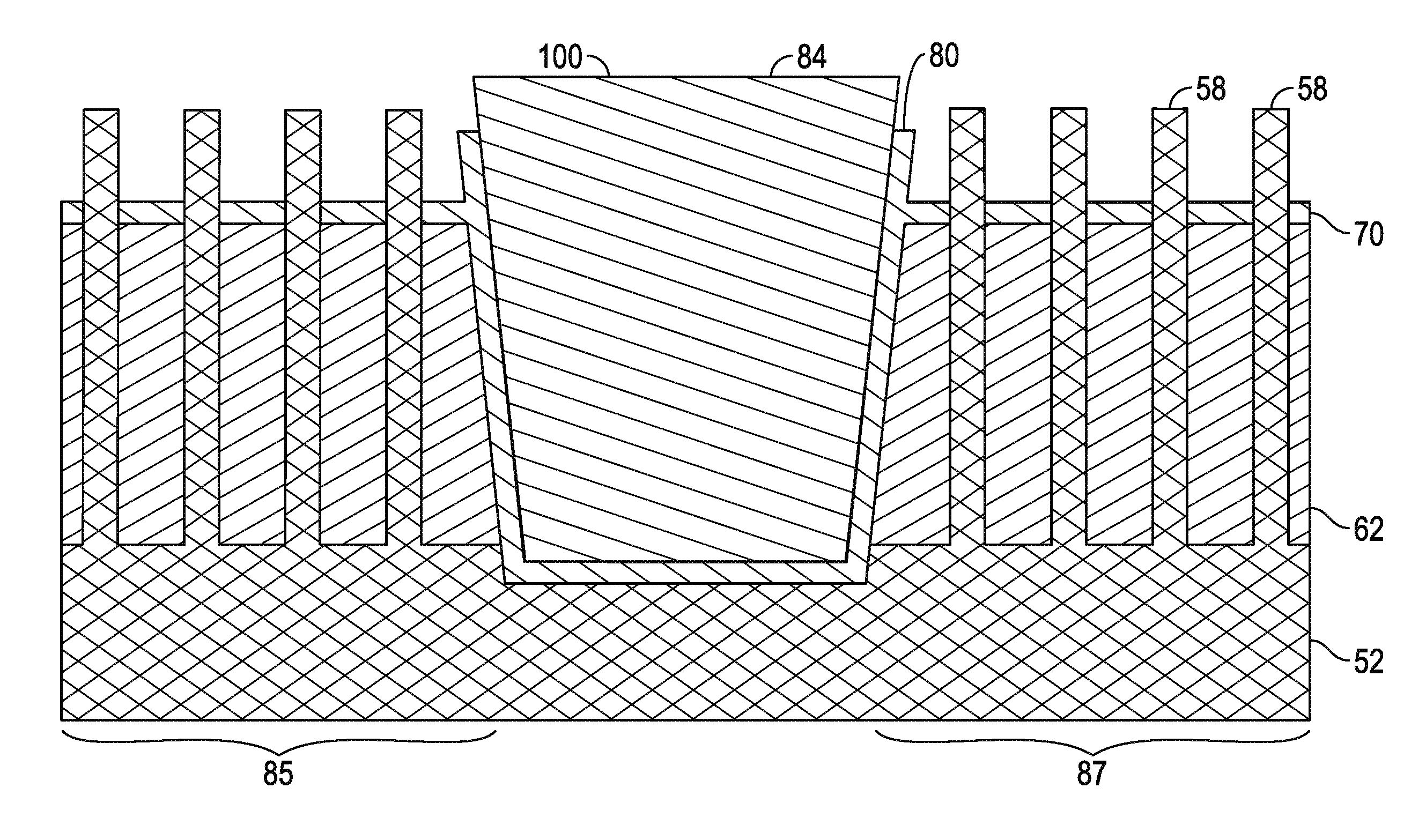
[0014]Various embodiments for methods of fabricating FinFET integrated circuits and FinFET integrated circuits made from such methods are provided herein. The methods utilize etch stop layers overlying a local isolation layer between the fins to maintain uniform fin height that ultimately controls the channel length and the resistance uniformity of the source and drain contacts. In addition, the methods use the etch stop layers to achieve shallow trench isolation (STI) that prevents lateral epitaxial growth on the fins that can result in shorting between adjacent devices. This in turn permits the design of narrower STI, thus providing additional substrate real estate for design flexibility....


PUM


Abstract

Methods for fabricating FinFET integrated circuits with uniform fin height and ICs fabricated from such methods are provided. A method includes etching a substrate using an etch mask to form fins. A first oxide is formed between the fins. A first etch stop is deposited on the first oxide. A second oxide is formed on the first etch stop. A second etch stop is deposited on the second oxide. A third oxide is deposited overlying the second etch stop. An STI extends from at least a surface of the substrate to at least a surface of the second etch stop overlying the fins to form a first active region and a second active region. The first etch stop overlying the fins is removed. The third oxide is removed to expose the second etch stop. A gate stack is formed overlying a portion of each of the fins.

Description

TECHNICAL FIELD[0001]The technical field generally relates to FinFET integrated circuits and methods for fabricating FinFET integrated circuits, and more particularly relates to FinFET integrated circuits with uniform fin height and methods for fabricating FinFET integrated circuits with uniform fin height.BACKGROUND[0002]To improve the operating speed of field effect transistors (FETs), and to increase the density of FETs on an integrated circuit device, device designers have greatly reduced the physical size of FETs over the years. More specifically, the channel length of FETs has been significantly decreased, which has resulted in improving the switching speed of FETs. However, decreasing the channel length of a FET also decreases the distance between the source region and the drain region. In some cases, this decrease in the separation between the source and the drain makes it difficult to efficiently inhibit the electrical potential of the source region and the channel from bei...

Claims


Application Information

Patent Timeline
Patent Type & Authority Applications(United States)
IPC IPC(8): H01L21/762H01L29/78
CPCH01L29/785H01L21/76224H01L29/66545H01L29/7851H01L27/0886H01L21/823431H01L29/66795
Inventor XIE, RUILONGCAI, XIUYU
Owner GLOBALFOUNDRIES US INC
Why Eureka
Try Eureka