Ultrasonic device, ultrasonic probe, electronic equipment, and ultrasonic imaging apparatus

a technology of ultrasonic elements and ultrasonic probes, applied in the direction of mechanical vibration separation, instruments, specific gravity measurement, etc., can solve the problems of ultrasonic elements or the substrates of ultrasonic elements being susceptible to damage, the structure of ultrasonic elements being disclosed, and the ultrasonic elements being susceptible to external forces. to achieve the effect of high reliability

Active Publication Date: 2014-07-31
SEIKO EPSON CORP
View PDF5 Cites 54 Cited by
  • Summary
  • Abstract
  • Description
  • Claims
  • Application Information

AI Technical Summary

Benefits of technology

[0042]The ultrasonic imaging apparatus of this application example includes the ultrasonic device that prevents damage to the ultrasonic element array substrate. Thus, it is possible to provide an ultrasonic imaging apparatus with high reliability.

Problems solved by technology

The structure of the ultrasonic elements disclosed in JP-A-2002-271897 is susceptible to damage by external forces, because of an opening provided in the substrate that is made of a brittle material.
In particular, such a structure suffers from a problem that, if an impact force is externally applied to an acoustic lens by being dropped or the like, the ultrasonic elements or the substrates of the ultrasonic elements are susceptible to damage.

Method used


Image

  • Ultrasonic device, ultrasonic probe, electronic equipment, and ultrasonic imaging apparatus
  • Ultrasonic device, ultrasonic probe, electronic equipment, and ultrasonic imaging apparatus
  • Ultrasonic device, ultrasonic probe, electronic equipment, and ultrasonic imaging apparatus

Examples


first embodiment

[0057]In this embodiment, an ultrasonic imaging apparatus for inspecting the inside of the human body is described as an example of electronic equipment.

[0058](1) Overall Configuration of Ultrasonic Imaging Apparatus

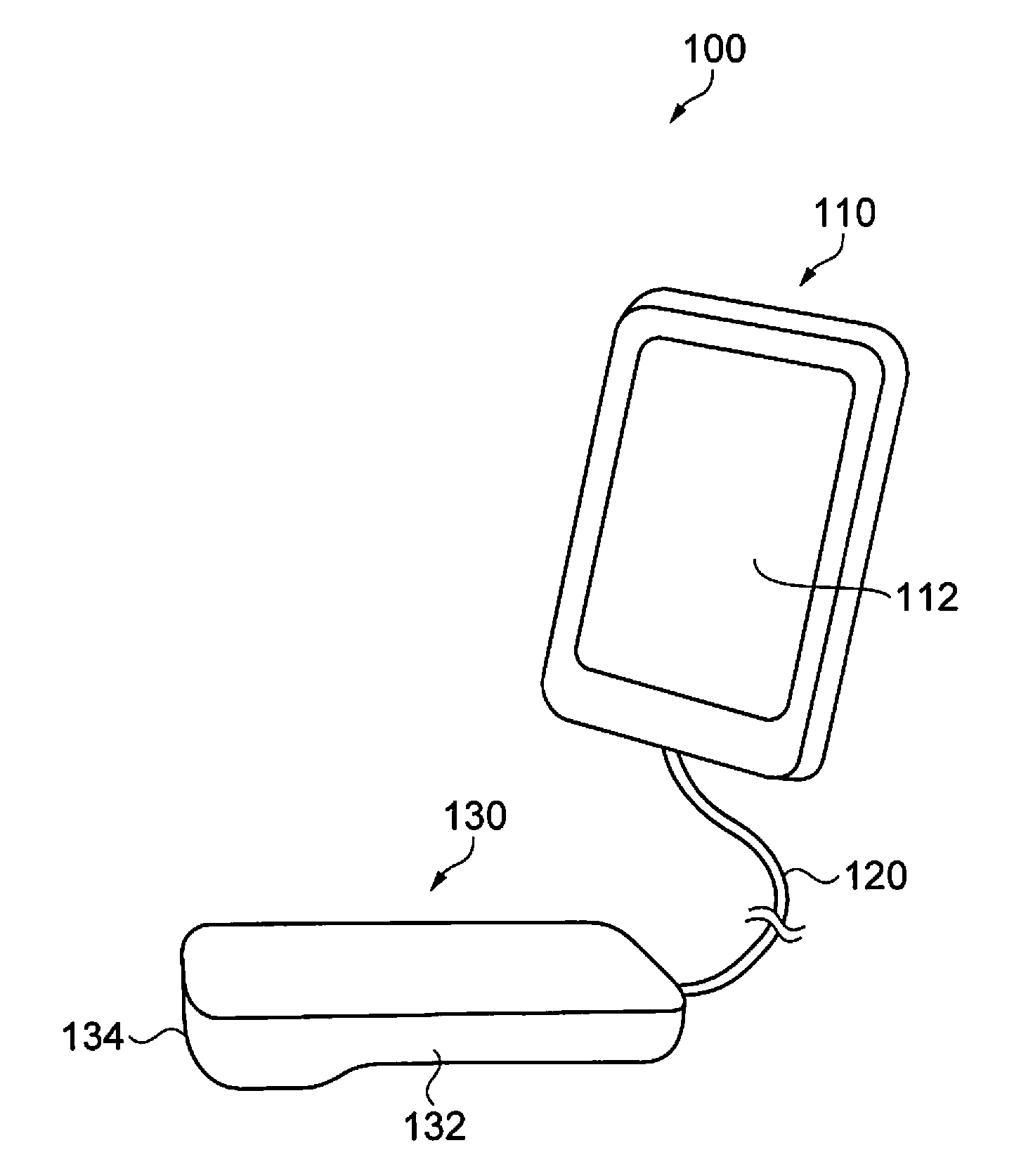
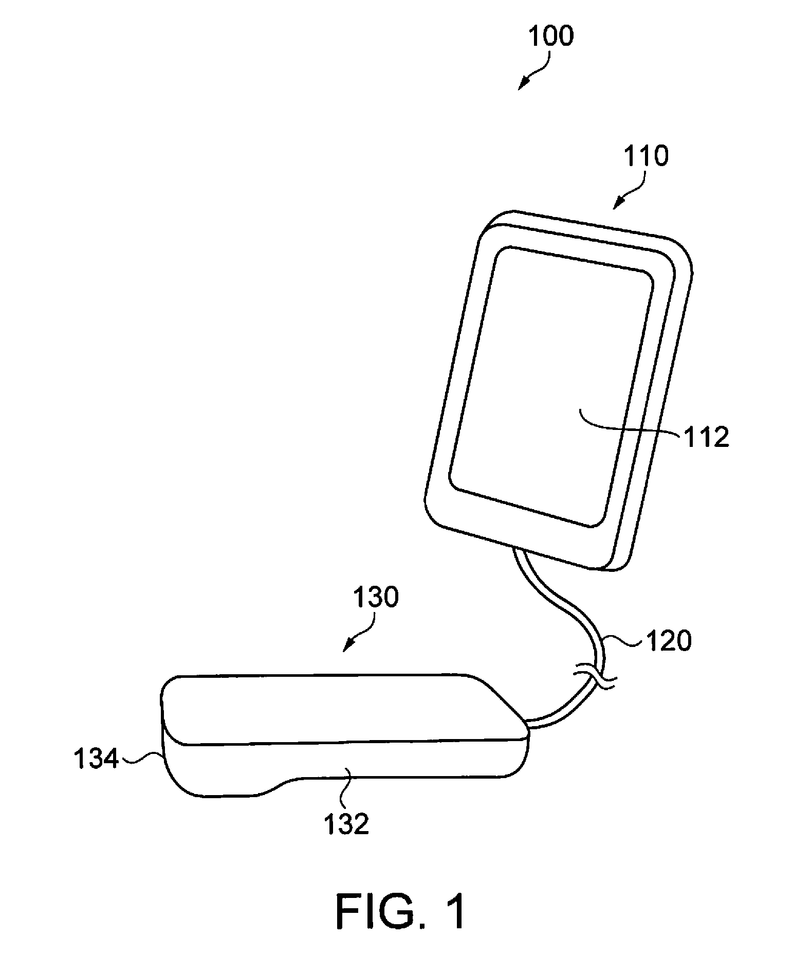
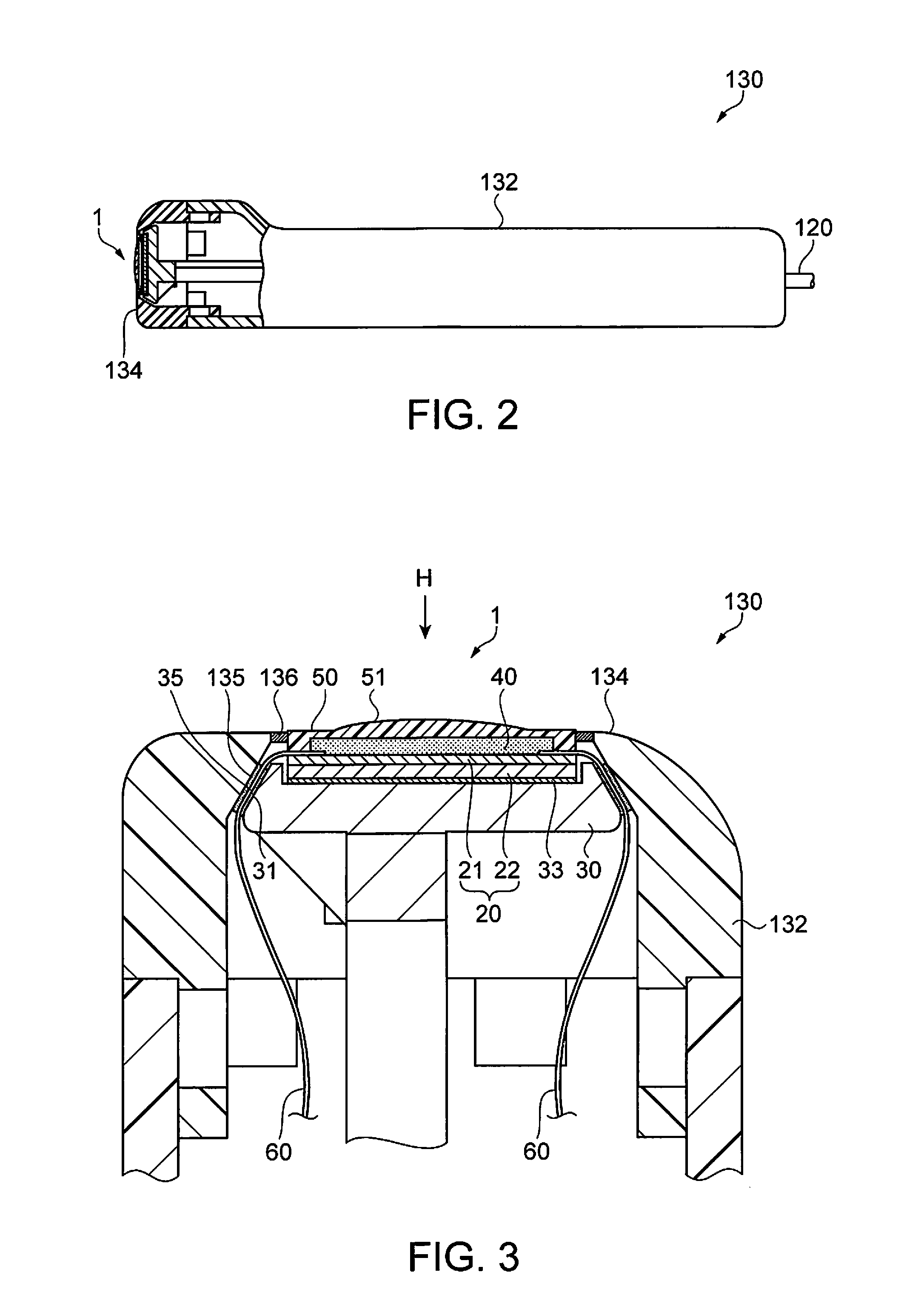
[0059]FIG. 1 shows a schematic outline of an ultrasonic imaging apparatus of this embodiment. FIG. 2 is a partial sectional view of an ultrasonic probe. FIG. 3 is an enlarged sectional view of a head portion of the ultrasonic probe.

[0060]As shown in FIG. 1, an ultrasonic imaging apparatus 100 includes an apparatus body 110 and an ultrasonic probe 130. The apparatus body 110 and the ultrasonic probe 130 are connected to each other by a cable 120. The apparatus body 110 and the ultrasonic probe 130 can exchange electrical signals via the cable 120.

[0061]The apparatus body 110 incorporates a display panel or the like as a display 112. In this embodiment, the display 112 is a touch panel display, and serves also as a user-interface unit (UI unit).

[0062]In the apparatus body ...


PUM

PropertyMeasurementUnit
thicknessaaaaaaaaaa
thicknessaaaaaaaaaa
frequencyaaaaaaaaaa

Abstract

Provided is an ultrasonic device including: an ultrasonic element array substrate having a plurality of ultrasonic elements that each include a piezoelectric body; an acoustic lens secured via an acoustic matching layer to a surface, formed with the ultrasonic elements, of the ultrasonic element array substrate; and a support member secured to a surface, opposite to the surface formed with the ultrasonic elements, of the ultrasonic element array substrate, wherein the support member is formed to have a larger area, in plan view in the thickness direction of the ultrasonic element array substrate, and a higher bending stiffness than the ultrasonic element array substrate, and the acoustic lens is formed to have a lower bending stiffness than the ultrasonic element array substrate. The above-described ultrasonic device further includes an acoustic matching layer filled between the ultrasonic element array substrate and the acoustic lens.

Description

BACKGROUND[0001]1. Technical Field[0002]The present invention relates to an ultrasonic device, an ultrasonic probe, electronic equipment, and an ultrasonic imaging apparatus.[0003]2. Related Art[0004]Up to the present time, ultrasonic elements that transmit and receive ultrasound have been known. For example, JP-A-2002-271897, which is an example of related art, discloses ultrasonic elements (ultrasonic transducers) each having a structure in which a substrate is provided with an opening, and a film, a first electrode, a piezoelectric layer, and a second electrode are sequentially layered over the opening. As the substrate of the ultrasonic elements, silicon substrates or the like are used. On such a silicon substrate, the first and second electrodes and the piezoelectric layer formed of thin films are provided.[0005]The structure of the ultrasonic elements disclosed in JP-A-2002-271897 is susceptible to damage by external forces, because of an opening provided in the substrate that...

Claims


Application Information

Patent Timeline
Patent Type & Authority Applications(United States)
IPC IPC(8): B06B3/04G01N29/06B06B1/06
CPCB06B3/04G01N29/0654B06B1/0622B06B3/00G10K11/30
Inventor ONISHI, YASUNORI
Owner SEIKO EPSON CORP
Why Eureka
Try Eureka