Method and device of a LED matrix

a technology of led matrix and led light, which is applied in the direction of lighting support devices, lighting and heating apparatus, laminated circuit boards, etc., can solve the problem of difficult wire mounting of small components, and achieve the effect of low cos

Active Publication Date: 2014-07-31
KONINKLIJKE PHILIPS ELECTRONICS NV
View PDF5 Cites 11 Cited by
  • Summary
  • Abstract
  • Description
  • Claims
  • Application Information

AI Technical Summary

Benefits of technology

[0010]According to an embodiment, the method further comprises providing at least one recess in the component area for receiving LEDs or LED packages of a size less then 1×1×1 mm, which is advantageous. This is applicable for Wafer Level Chip Scale Package, WLCSP, which are expected to become the lowest cost package for LED's on the market.
[0011]According to an embodiment, the step of mounting comprises defining solder areas on the first conductor structure, applying solder onto the solder areas, placing the LEDs on a respective component area, and performing soldering, which is advantageous.

Problems solved by technology

However, mounting of small components is difficult on wires, and the proposed method requires that the wires have to be placed on a temporary carrier which is removed after mounting of the components.

Method used


Image

  • Method and device of a LED matrix
  • Method and device of a LED matrix
  • Method and device of a LED matrix

Examples


Embodiment Construction

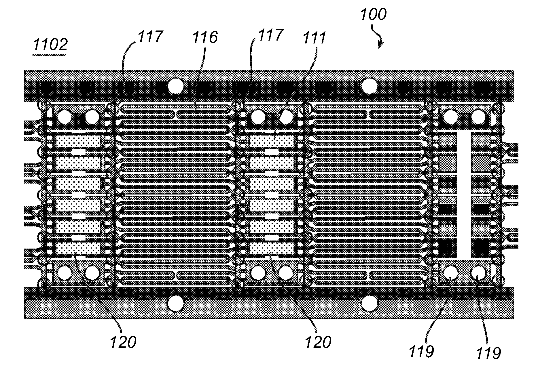
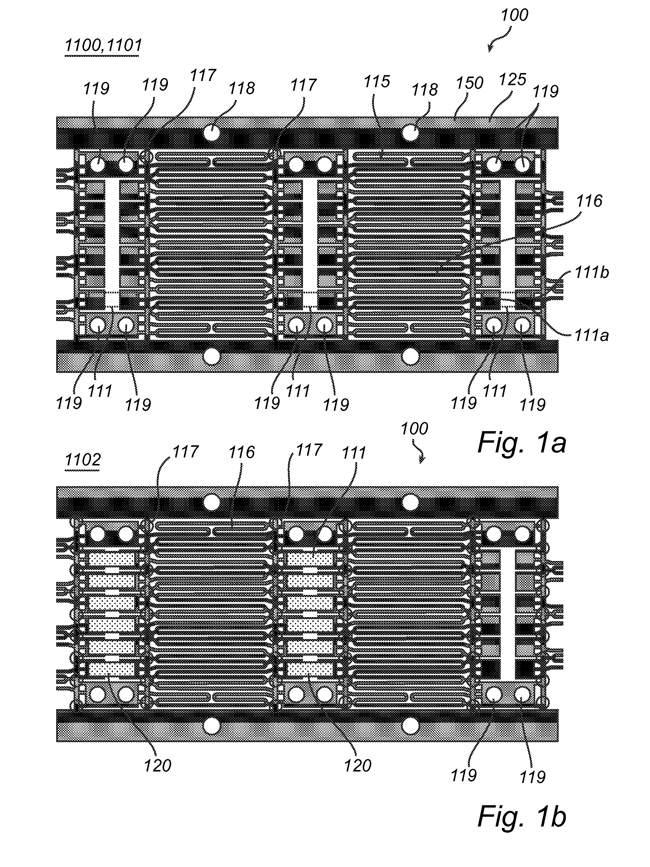
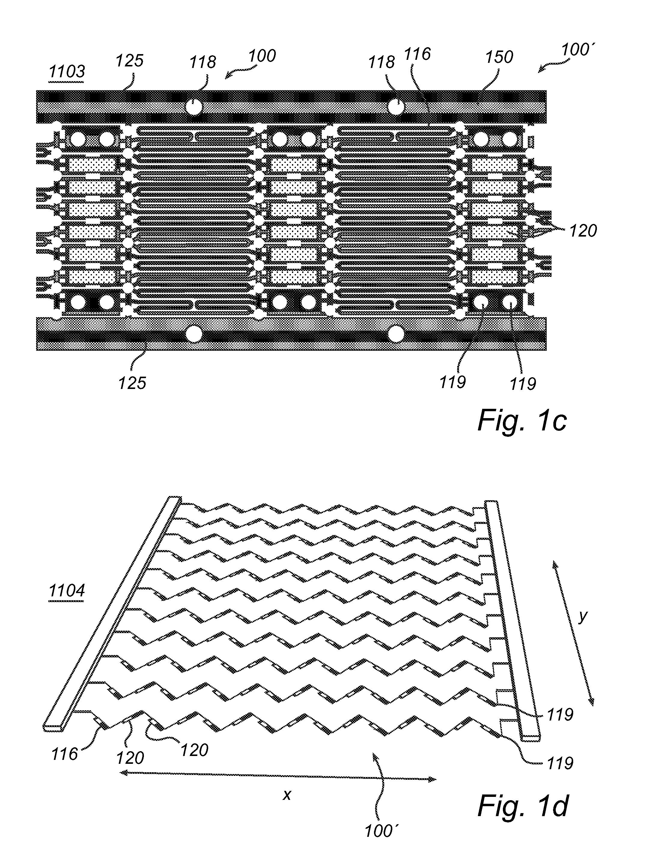
[0023]An exemplifying embodiment of the method for manufacturing a LED matrix according to the present invention is now described with reference to FIGS. 1a)-e). The steps of the method are described as a continuous sequence, however some of the steps may be performed in another order or some additional process step may be interleaved. The conductor structure in the LED matrix is also referred to as a lead frame herein under.

[0024]With reference now to FIG. 1a), and starting at a step [1100] of the method, a conductor sheet 150 is initially provided. The conductor sheet is preferably selected amongst a group of metal sheet materials comprising Cu, Cu / Ni, Ni / Fe, Cu plated Fe, Cu plated RVS (stainless steel), tin plated Fe, and metal plated polymers. The conductor sheet 150 is here a 200 μm thick copper sheet.

[0025]A first predetermined pattern 115 is at a step [1101] applied to the conductor sheet 150, thereby forming a first conductor structure 100, which corresponds to a specific m...


PUM

PropertyMeasurementUnit
sizeaaaaaaaaaa
thickaaaaaaaaaa
lengthaaaaaaaaaa

Abstract

There is provided a method for manufacturing a light emitting diode, LED, matrix (100) comprising the steps of providing with a maintained integrity a conductor sheet (150) with a plurality of component areas (111) interconnected with meandering connection tracks (116), mounting a plurality of LEDs (120) to a respective component area thereby forming a subassembly (100″), trimming and stretching the subassembly thereby straightening the connection tracks such that an m×n LED conductor matrix is formed during the step of stretching.

Description

FIELD OF THE INVENTION[0001]The present invention relates to the field of light emitting diode (LED) lighting devices, and more particularly to a method for manufacturing a light emitting diode, LED, matrix for large area LED lighting devices, and a corresponding lighting device.BACKGROUND OF THE INVENTION[0002]Light emitting diodes (LEDs) in large area lighting devices have been used for some time, where a large number of LEDs are arranged as an array or matrix to evenly provide lighting over a large area. Typically, LEDs have been arranged on a printed circuit board (PCB) by means of traditional surface mounting techniques. However, recently there has been proposed other types of solutions to provide large area LED arrays.[0003]WO 2007 / 125566 A1 discloses a method for manufacturing a LED array in which N electrically conducting wires are arranged in parallel creating an array of wires having a width D perpendicular to the length direction of the wires. Further, LED components are ...

Claims


Application Information

Patent Timeline
Patent Type & Authority Applications(United States)
IPC IPC(8): H01L27/15H01L33/62
CPCH01L33/62H01L27/153H05K1/0283H05K3/202H05K2201/09263H05K2201/10106H05K2203/1545H01L25/0753H01L2924/0002H05K13/046H05K1/05Y10T29/49144H01L2924/00H05K1/0209H05K1/0284H05K3/0058H05K3/0097H05K2201/09781H05K2203/175F21K9/90F21V21/002H05K3/303H05K2203/04
Inventor DINGEMANS, ANTONIUS PETRUS MARINUSWEEKAMP, JOHANNES WILHELMUSLIBON, SEBASTIEN PAUL RENEKUMS, GERARDCENNINI, GIOVANNI
Owner KONINKLIJKE PHILIPS ELECTRONICS NV
Why Eureka
Try Eureka