N-channel double diffusion mos transistor, and semiconductor composite device

Active Publication Date: 2014-07-31
ROHM CO LTD
View PDF9 Cites 12 Cited by
  • Summary
  • Abstract
  • Description
  • Claims
  • Application Information

AI Technical Summary

Benefits of technology

The present invention provides an n-channel double diffusion MOS transistor with excellent switching characteristics and a semiconductor composite device including the n-channel double diffusion MOS transistor. This results in improved performance and reliability of the semiconductor device.

Problems solved by technology

This makes it difficult to provide excellent switching characteristics.
Since the p-type body layer is surrounded by the n-type well, a depletion layer cannot sufficiently laterally spread, making it impossible to reduce the ON resistance.

Method used


Image

  • N-channel double diffusion mos transistor, and semiconductor composite device
  • N-channel double diffusion mos transistor, and semiconductor composite device
  • N-channel double diffusion mos transistor, and semiconductor composite device

Examples


Embodiment Construction

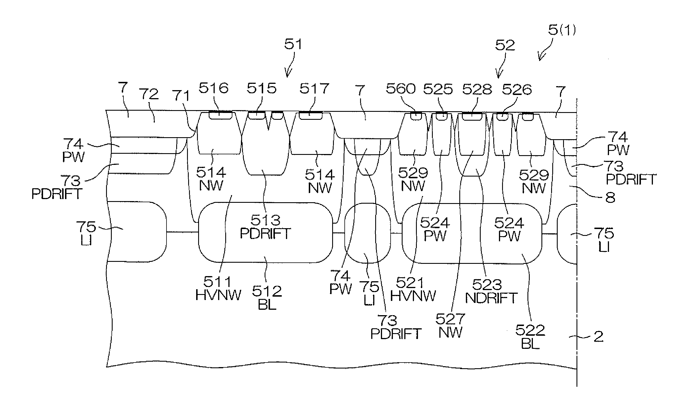
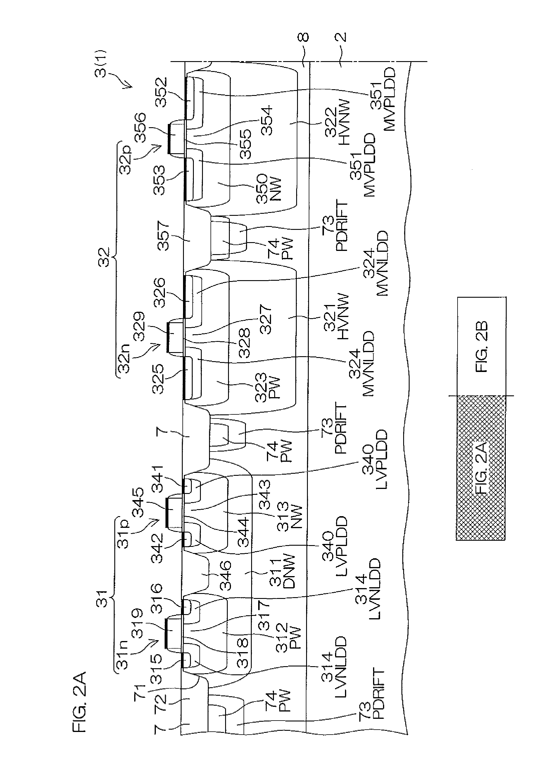
[0015]According to an embodiment of the present invention, there is provided an n-channel double diffusion MOS transistor, which includes: a p-type semiconductor substrate; a p-type epitaxial layer formed on the p-type semiconductor substrate through epitaxial growth; an n-type buried layer provided in a boundary between the p-type semiconductor substrate and the p-type epitaxial layer; a p-type body layer provided in a surface portion of the p-type epitaxial layer; an n-type source layer provided in the p-type body layer and defining a double diffusion structure together with the p-type body layer; an n-type drift layer provided in a surface portion of the p-type epitaxial layer in spaced relation from the p-type body layer to define a channel region between the n-type source layer and the n-type drift layer; an n-type drain layer provided in a surface portion of the p-type epitaxial layer in spaced relation from the channel region and in contact with the n-type drift layer; a p-ty...


PUM


Abstract

The n-channel double diffusion MOS transistor includes a p-type semiconductor substrate, a p-type epitaxial layer, and an n-type buried layer provided in a boundary between the p-type semiconductor substrate and the p-type epitaxial layer. In a p-type body layer provided in a surface portion of the p-type epitaxial layer, an n-type source layer is provided to define a double diffusion structure together with the p-type body layer. An n-type drift layer is provided in a surface portion of the p-type epitaxial layer in spaced relation from the p-type body layer. An n-type drain layer is provided in a surface portion of the p-type epitaxial layer in contact with the n-type drift layer. A p-type buried layer having a lower impurity concentration than the n-type buried layer is buried in the p-type epitaxial layer between the n-type drift layer and the n-type buried layer in contact with an upper surface of the n-type buried layer.

Description

BACKGROUND OF THE INVENTION[0001]1. Field of the Invention[0002]The present invention relates to an n-channel double diffusion MOS (Metal Oxide Semiconductor) transistor, and a semiconductor composite device including the same.[0003]2. Description of Related Art[0004]US2010 / 0051946A1 discloses a BiCDMOS (Bipolar CMOS DMOS) device which is a semiconductor composite device including a bipolar element, a CMOS (Complementary MOS) transistor and a DMOS (Double Diffusion MOS) transistor provided on a common semiconductor substrate. An n-channel DMOS transistor generally has an n-type well provided on a p-type semiconductor substrate with the intervention of an n-type buried layer. In a surface portion of the n-type well, a p-type body layer and an n-type drift layer are provided in spaced relation, and a channel region is defined between the p-type body layer and the n-type drift layer. An n-type source layer is provided in the p-type body layer. In the n-type well, an n-type drain layer ...

Claims


Application Information

Patent Timeline
IPC IPC(8): H01L29/78H01L27/06
CPCH01L27/0623H01L29/7825H01L21/823814H01L21/823892H01L21/8249H01L27/0635H01L29/665H01L29/7833H01L29/1083H01L28/10H01L28/40H01L29/7816H01L27/0922H01L29/0865H01L29/1095
Inventor SAWASE, KENSUKETOYONAGA, MOTOHIRO
Owner ROHM CO LTD
Why Eureka
Try Eureka