Surface potential measuring apparatus and surface potential measuring method

a technology of surface potential and measuring apparatus, which is applied in the direction of semiconductor/solid-state device testing/measurement, instruments, material analysis, etc., can solve the problems of low accuracy of surface potential measurement, short circuit between the interconnects or leakage of current, and poor adhesion between the copper interconnects and the dielectric film. achieve the effect of accurate measurement of surface potential of the object and low pri

Active Publication Date: 2014-09-11
EBARA CORP
View PDF9 Cites 2 Cited by
  • Summary
  • Abstract
  • Description
  • Claims
  • Application Information

AI Technical Summary

Benefits of technology

[0017]According to the above-described embodiments, the electric potential measuring device is calibrated based on the measured value of the surface potential of the reference structure before measuring the surface potential of the object. Since the reference structure has the same construction as the underlying structure lying under the object, the surface potential of the underlying structure is cancelled by the calibration. Therefore, the electric potential measuring device can accurately measure the surface potential of the object through the probe. Elements that constitute the apparatus, including the probe and the electric potential measuring device, can be available at low prices on the market. Therefore, it is possible to provide the surface potential measuring apparatus with a low price.

Problems solved by technology

The electrostatic charge of the substrate surface may cause reattachment of particles that have been once removed by the cleaning process of the substrate surface, and may cause destruction of devices due to electrostatic discharge.
Consequently, shortcut between the interconnects or leakage of current may occur, and / or poor adhesion between the copper interconnects and the dielectric film may occur.
Since the electrostatic charge of the substrate surface can lower a reliability of the devices, it is necessary to measure an amount of static electricity, i.e., a surface potential, and monitor it.
However, a conventional device for measuring the surface potential of the substrate is very expensive.
As a result, device fabrication costs will increase.
Consequently, it has been difficult to precisely measure an accurate surface potential so far.

Method used


Image

  • Surface potential measuring apparatus and surface potential measuring method
  • Surface potential measuring apparatus and surface potential measuring method
  • Surface potential measuring apparatus and surface potential measuring method

Examples


Embodiment Construction

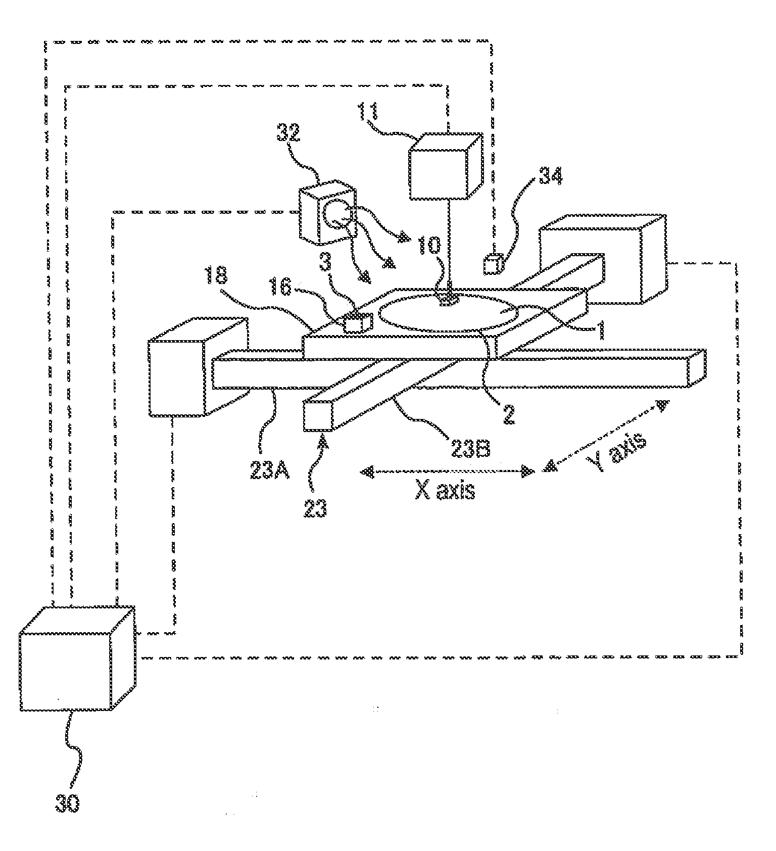
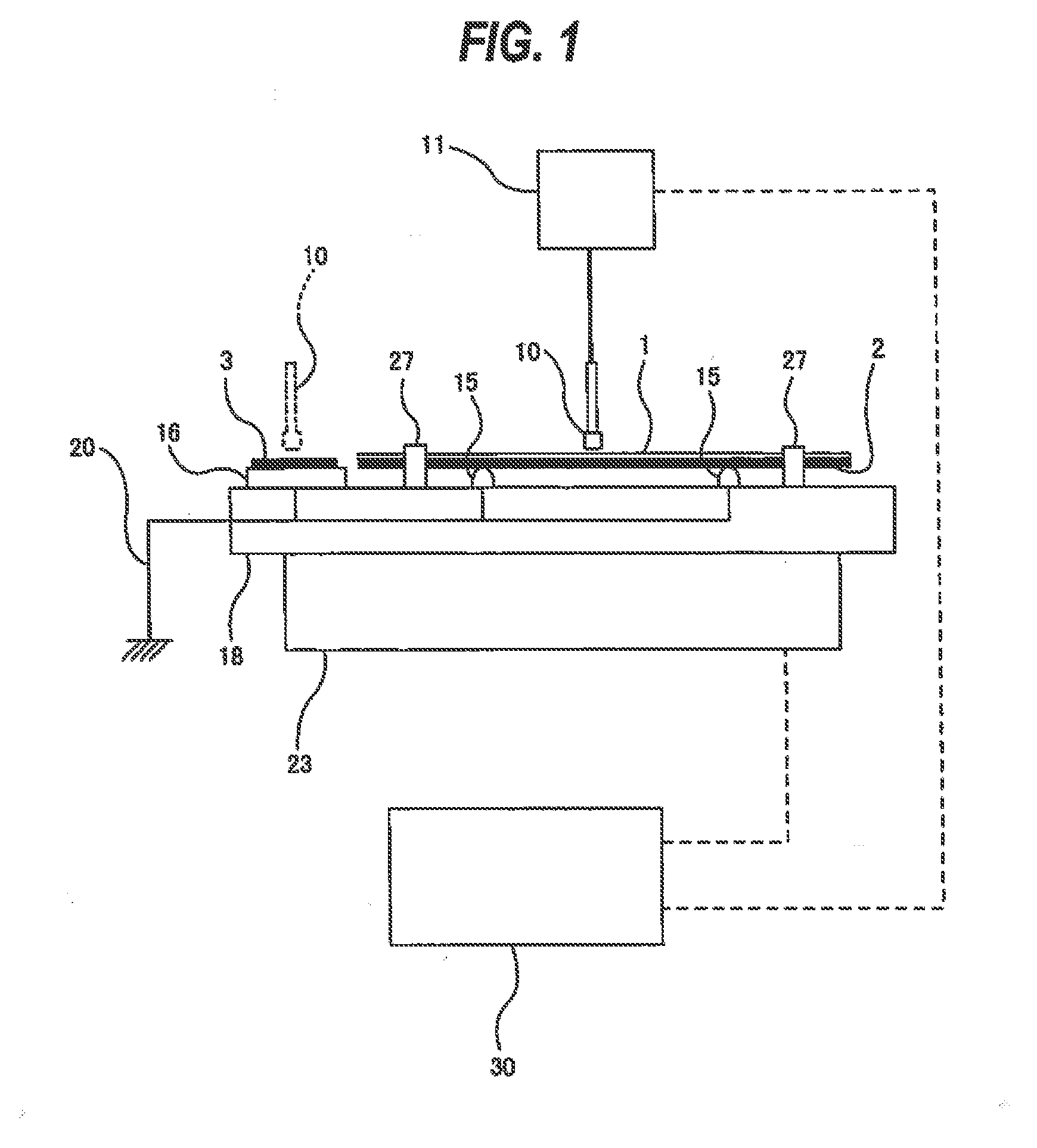
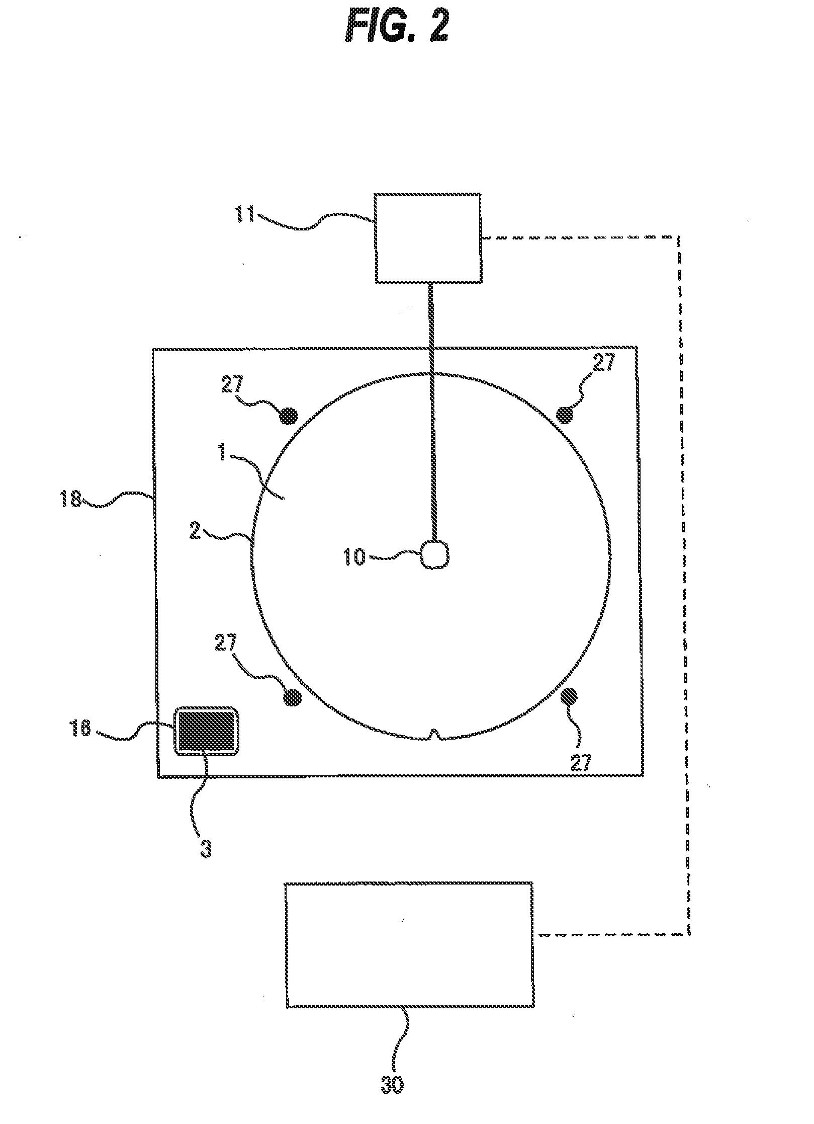
[0023]An embodiment will be described below with reference to the drawings. FIG. 1 is a side view showing an embodiment of a surface potential measuring apparatus, and FIG. 2 is a plan view showing the surface potential measuring apparatus. The surface potential measuring apparatus includes a probe 10, an electric potential measuring device 11 coupled to the probe 10, a first support member 15 for supporting an underlying structure 2 on which a film 1 (which is an object to be measured) is formed, and a second support member 16 for supporting a reference structure 3. The first support member 15 and the second support member 16 are secured to an upper surface of a measurement table 18.

[0024]The underlying structure 2 may be a silicon substrate having a diameter ranging from 25 mm to 450 mm. The object to be measured may be a dielectric film or a device having a dielectric film and metal interconnects formed on the silicon substrate. For example, the underlying structure 2 shown in FI...


PUM

PropertyMeasurementUnit
diameteraaaaaaaaaa
surface potentialaaaaaaaaaa
distanceaaaaaaaaaa

Abstract

An apparatus for measuring a surface potential of an object on an underlying structure is disclosed. A relatively-moving mechanism moves a probe and a second support member relative to each other until the probe faces a reference structure on the second support member, an electric potential measuring device measures the surface potential of the reference structure through the probe, the controller calibrates the electric potential measuring device such that a measured value of the surface potential of the reference structure becomes 0, the relatively-moving mechanism moves the probe and a first support member relative to each other until the probe faces the object on the first support member after the calibration, and the electric potential measuring device measures the surface potential of the object through the probe.

Description

CROSS REFERENCE TO RELATED APPLICATION[0001]This document claims priority to Japanese Patent Application No. 2013-44267 filed Mar. 6, 2013, the entire contents of which are hereby incorporated by reference.BACKGROUND[0002]In a manufacturing process of a semiconductor device, various films having different physical properties are formed on a silicon substrate and these films are subjected to various processes, thus forming fine metal interconnects. For example, in a damascene interconnect forming process, interconnect trenches are formed in a film, and the interconnect trenches are then filled with metal. Thereafter, an unnecessary metal is removed by chemical mechanical polishing (CMP), so that metal interconnects are formed. A variety of films including a metal film, a barrier film, and a dielectric film exist on a surface of the substrate that has been manufactured through such a damascene interconnect forming process.[0003]A CMP apparatus (polishing apparatus) for polishing a sub...

Claims


Application Information

Patent Timeline
Patent Type & Authority Applications(United States)
IPC IPC(8): G01N27/60
CPCH01L22/00G01R29/12G01R31/2831H01L22/14H01L2924/0002H01L2924/00
Inventor ISHIBASHI, TOMOATSU
Owner EBARA CORP
Why Eureka
Try Eureka