High accuracy electrical test interconnection device and method for electrical circuit board testing

a high-accuracy, interconnection device technology, applied in measurement devices, printed circuit testing, instruments, etc., can solve the problems of increasing the difficulty and cost of traditional manufacturing methods, the deviation of the probe tip from the intended target pad, and the mechanical complexity of the probe, so as to improve the reliability of the fixture, simplify the maintenance and board interchange operation, and the effect of higher accuracy

Active Publication Date: 2014-09-11
DEMILLE DONALD
View PDF5 Cites 8 Cited by
  • Summary
  • Abstract
  • Description
  • Claims
  • Application Information

AI Technical Summary

Benefits of technology

[0014]However, with the new method of testing described herein, all of the replaceable fixture hardware for each different circuit board can be captured in the plastic tester interface transfer block, simplifying the maintenance and board interchange operations and increasing the reliability of the fixture by protecting the electrical elements within the transfer block. Because of the versatility of three dimensional printing, specialized shape target probes can be used in place of the cylindrical target probes. This has the advantage of providing access to test pad types that may not have been accessible using cylindrical probes.
[0015]The use of three dimensional printing in the instant invention enables higher accuracy probing of smaller and denser test pads during ICT or bare board testing of printed circuit boards. With three dimensional printing, more complex shapes can be created at a lower cost with less specialized machinery, dramatically simplifying the production process. The high resolution and accuracy of the three dimensional printing allows for increased positional accuracy of the target probes. This invention also minimizes the need for complex wiring or soldering operations during the fixture assembly process.

Problems solved by technology

Any misalignment in the vertical dimension can cause the probe tip to deviate from intended target pad.
To maintain vertical alignment as test pad sizes decrease has become increasingly more difficult and expensive using traditional manufacturing methods.
These probes are mechanically complex and expensive, containing a socket, a probe tip and an internal spring to apply force to the test pad.
Because of the length of the probe relative to the size of the target test pad, any deviation from the vertical translates into a positional error that makes it difficult and expensive to access smaller target test pads.

Method used


Image

  • High accuracy electrical test interconnection device and method for electrical circuit board testing
  • High accuracy electrical test interconnection device and method for electrical circuit board testing
  • High accuracy electrical test interconnection device and method for electrical circuit board testing

Examples


Embodiment Construction

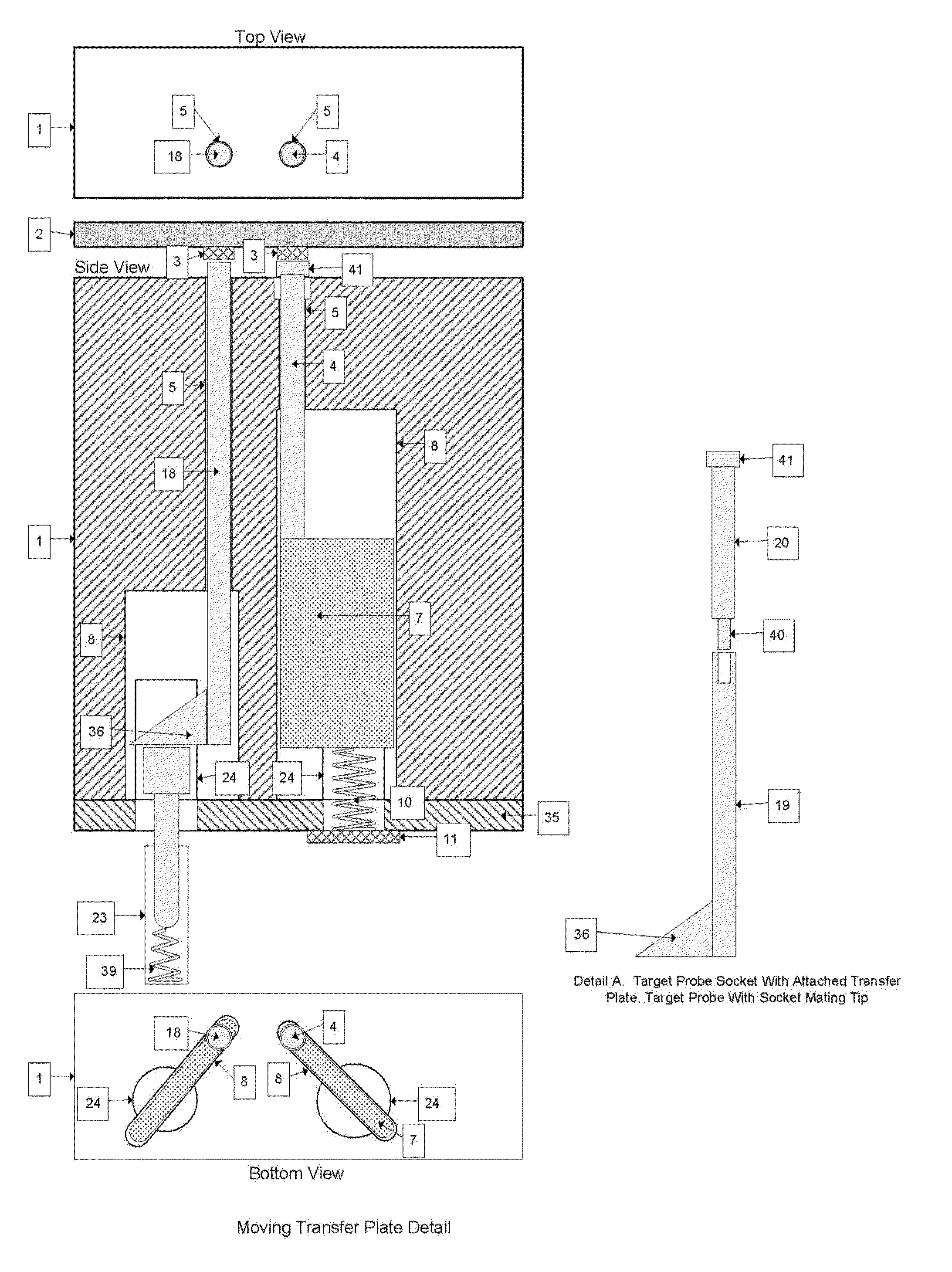
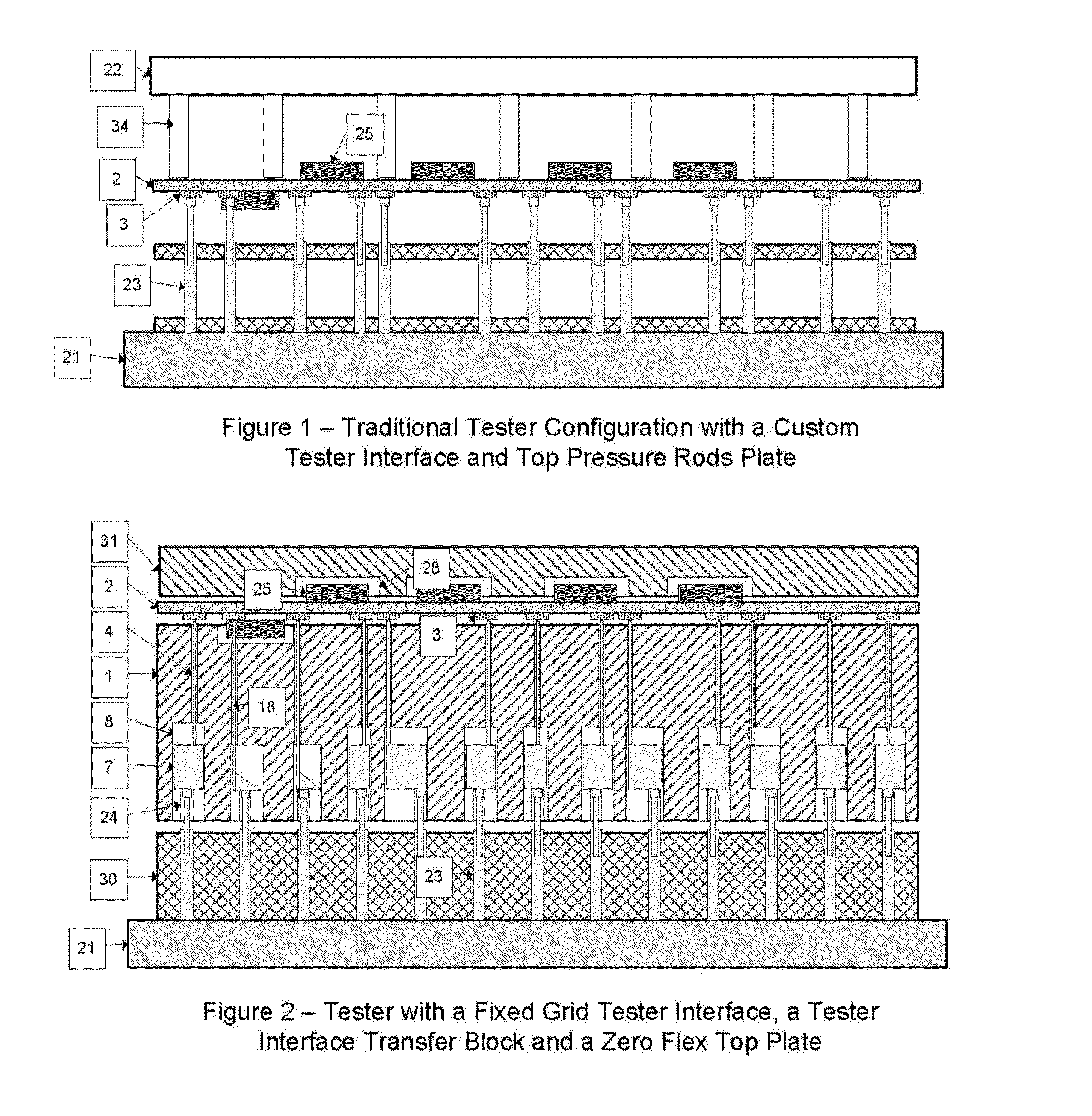
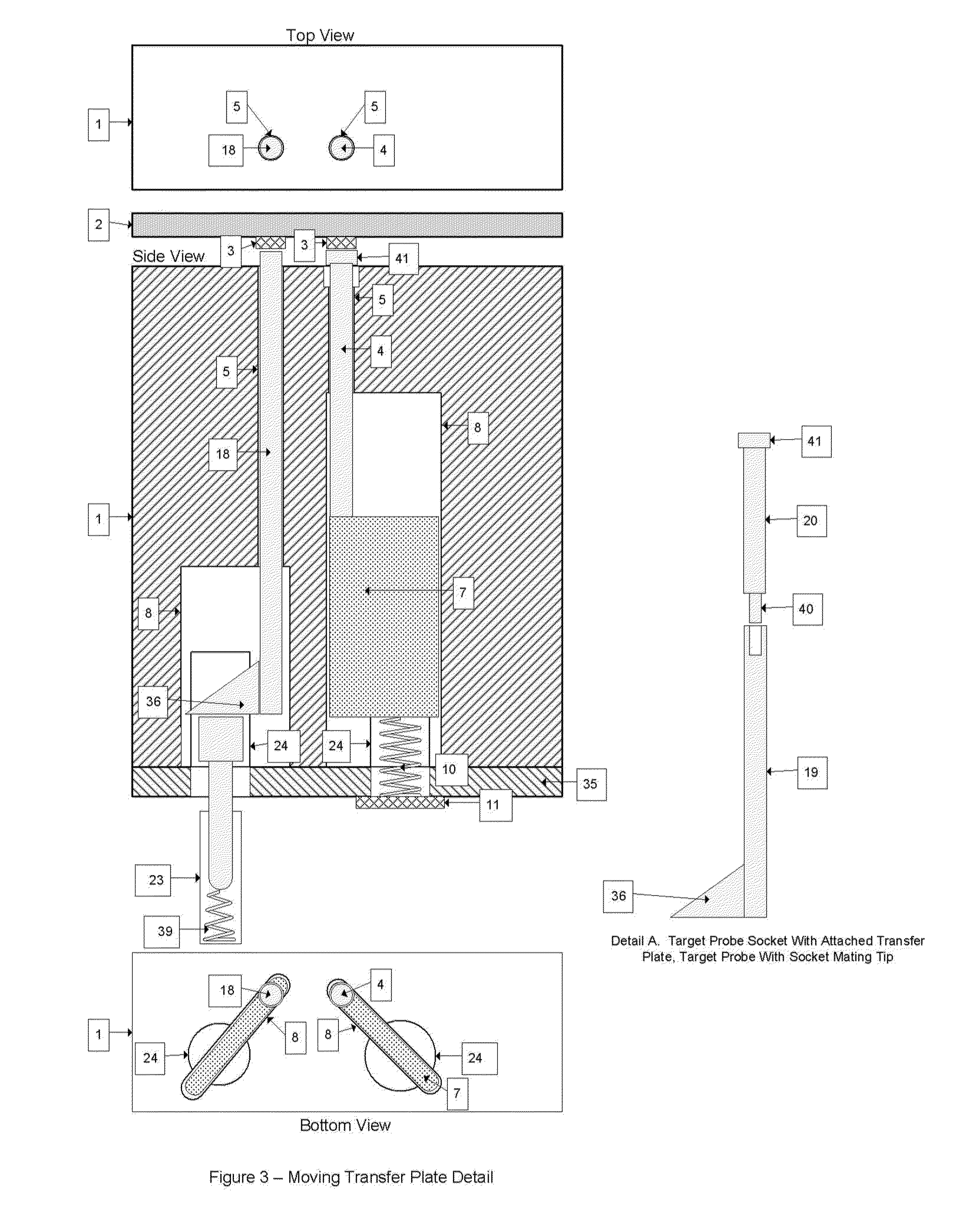
[0033]At the heart of this invention is the three dimensional tester interface transfer block. The tester interface transfer block is preferably fabricated using three dimensional printing technology. A specially designed software package (“the software”) is used to automatically create tubes and slots in the plastic tester interface transfer block. To begin the design process, Computer Aided Design (“CAD”) information for the circuit board to be tested is loaded into the software. With this CAD information, the software will determine the relevant circuit board target test pad locations. From there, the appropriate standard tester interface with corresponding tester resource contacts is chosen.

[0034]Once the tester resource contacts and target test pad locations are defined, the software determines the location of the closest unused tester resource to each target test pad. During this process, the software will resolve overlapping transfer plates issues using a variety of methods i...


PUM


Abstract

A high accuracy electrical test interconnect method employs a tester interface transfer block to enable the transfer of electrical contact from less accurate tester resource probes to target probes which are contained in the tester interface transfer block and can be positioned with high accuracy using the three dimensional printing to enable reliable contact with smaller test pads. The target probes can directly contact the tester resource probes or a transfer plate can be interposed between the target probes and the tester resource probes to allow positional adjustment of the target probes relative to the tester resource probes. This invention also includes the use of specialized shape target probes that can contact circuit board objects, such as vertical conductive surfaces and irregular shape test pads that have not been accessible with traditional methods.

Description

[0001]This application claims the benefit of U.S. Provisional Patent Application No. 61 / 775,072 filed on Mar. 8, 2013. The disclosure of the referenced application is hereby incorporated herein in its entirety by reference.[0002]The present invention relates to the field of fabricating electronic interconnections from a tester to a circuit board for the purpose of testing the electrical characteristics of the circuit board.[0003]In-Circuit (ICT) or bare board testing of printed circuit boards is used to perform tests on printed circuit assemblies during the assembly phase. The general purpose of this testing is to find component and manufacturing problems with the boards before the full assembly is complete. ICT uses multiple probes to make electrical connections between a tester and various points on the circuit board being tested for the purpose of measuring the electrical characteristics of the board. This verification method tests the individual components of the circuit board a...

Claims


Application Information

Patent Timeline
Patent Type & Authority Applications(United States)
IPC IPC(8): G01R1/067
CPCG01R1/067G01R1/07328G01R31/2808
Inventor DEMILLE, DONALD
Owner DEMILLE DONALD
Why Eureka
Try Eureka