
Advanced semiconductor-conductor composite particle structures for solar energy conversion

a composite particle and semiconductor technology, applied in the direction of energy input, electrical-based machining electrodes, manufacturing tools, etc., can solve the problems of low charge separation yield, high-efficiency solar cells (e.g. si, gaas) are also the most expensiv

Inactive Publication Date: 2014-09-18
RES TRIANGLE INST +3
View PDF3 Cites 16 Cited by
  • Summary
  • Abstract
  • Description
  • Claims
  • Application Information

AI Technical Summary

Benefits of technology

This patent describes an electrode for solar conversion that includes a porous structure with electrically conductive nanoparticles. The nanoparticles are surrounded by a meandering electrical path that connects them together. The electrode has a semiconductive coating with a thickness less than 200 nm that is conformal on the nanoparticles. The semiconductive coating can be made of various materials such as tin oxide, chromophore, and transition metals. The electrode has a high surface area in a range between 5 and 400 m2 / gm. The nanoparticles can be made of various materials such as zinc-doped tin oxide, tin-doped indium oxide, and graphene. The electrode can be used in a solar conversion device.

Problems solved by technology

In the fifty years since their arrival to the marketplace, there still exists an unfortunate tradeoff: high efficiency solar cells (e.g. Si, GaAs) are also the most costly.
The high cost stems from the need for high purity semiconductors and materials that minimize the recombination of free carriers (holes and electrons) that are created upon light absorption; higher defect densities result in lower charge separation yields due to recombination.

Method used


Image

  • Advanced semiconductor-conductor composite particle structures for solar energy conversion
  • Advanced semiconductor-conductor composite particle structures for solar energy conversion
  • Advanced semiconductor-conductor composite particle structures for solar energy conversion

Examples


Embodiment Construction

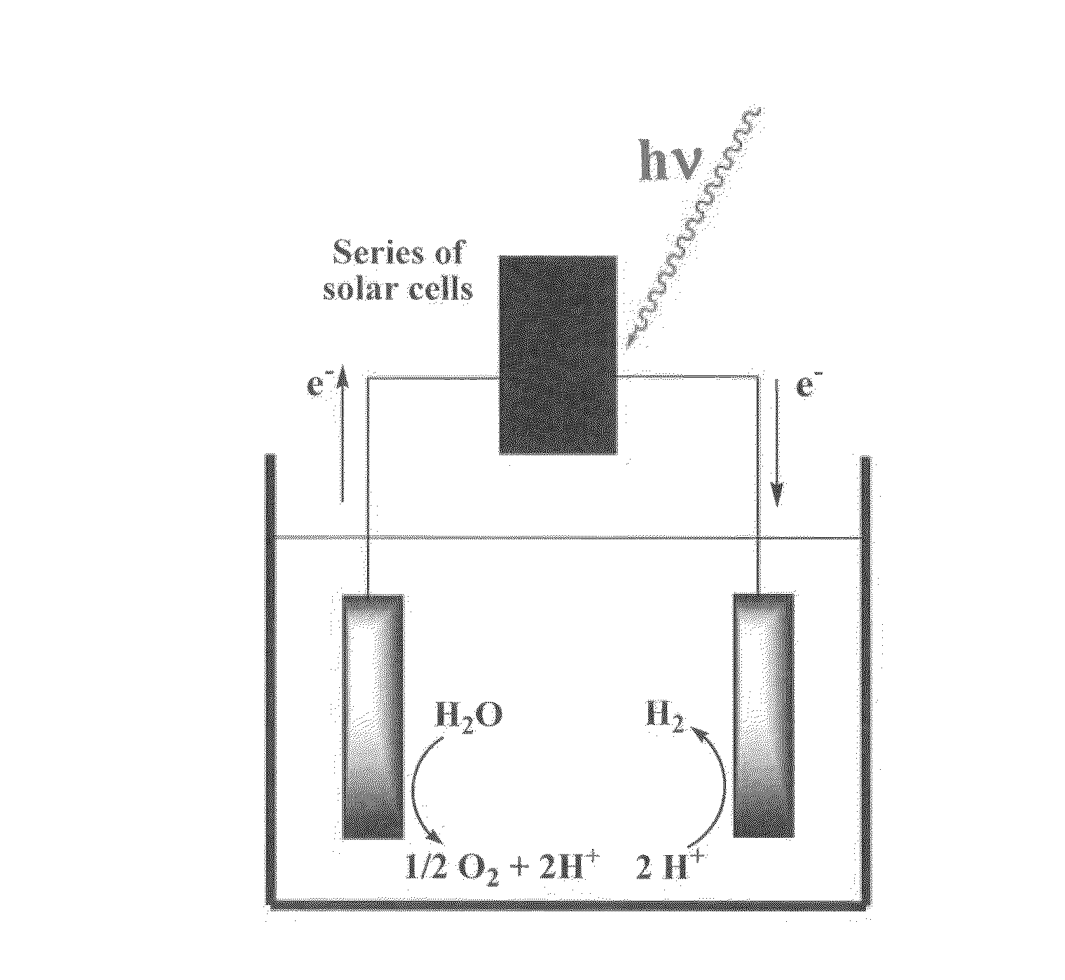
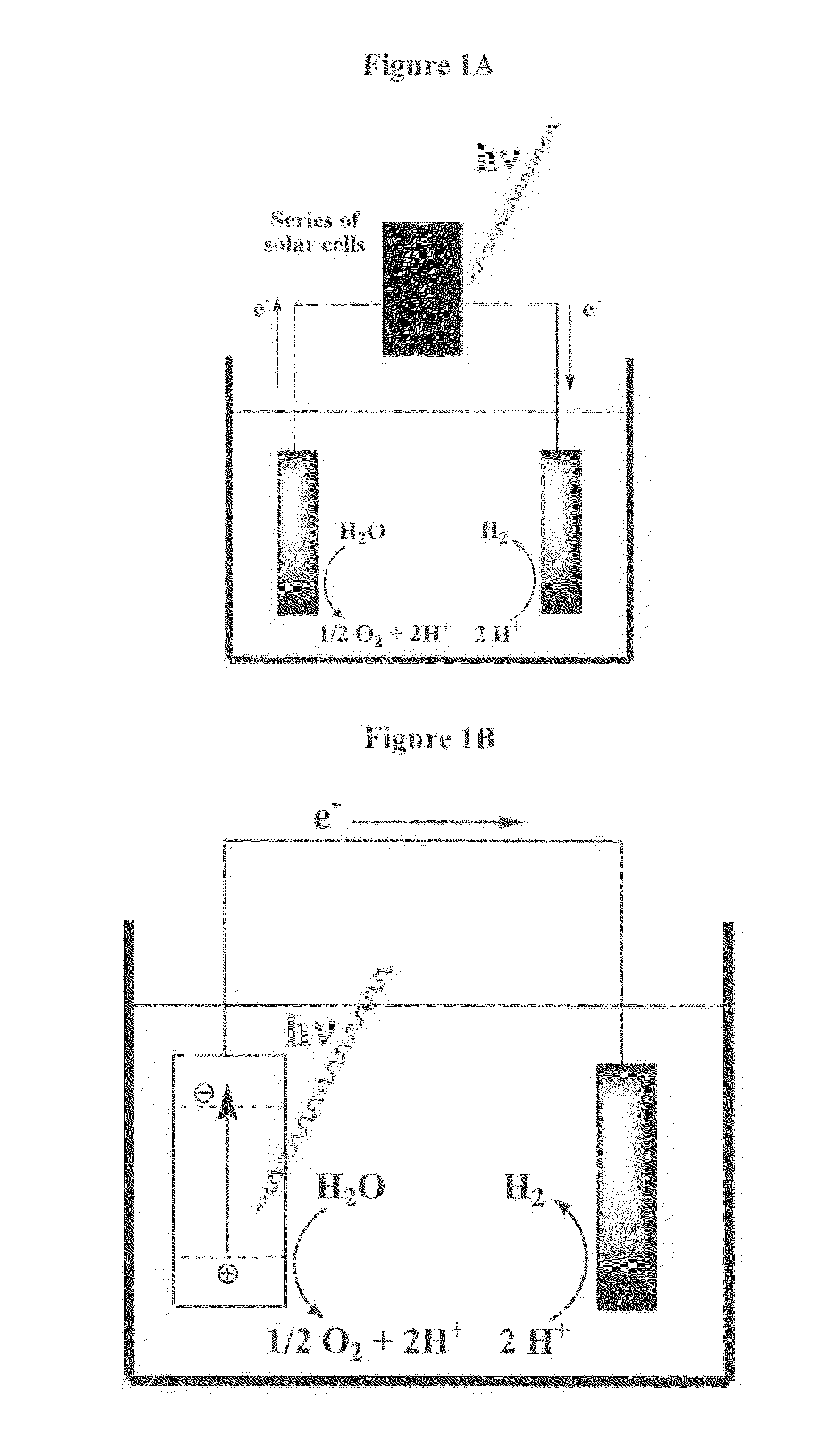
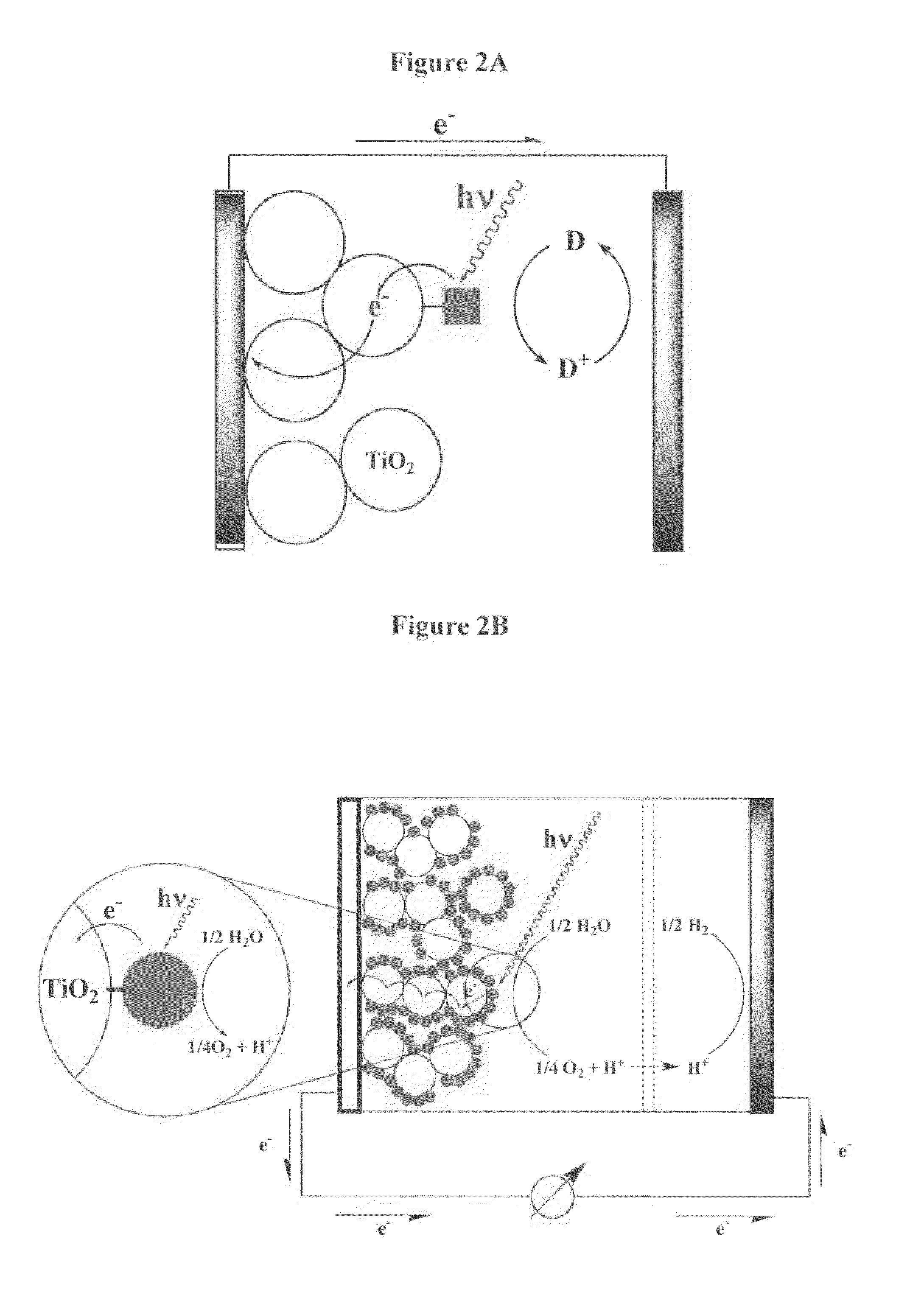
[0027]The invention in one aspect provides conformal nanoscale coatings onto pre-assembled, three dimensional objects for the creation of multi-component composites. In one example, a semiconductor coated consolidated conducting nanoparticle structure provides a unique structure for electron transport and utilization where electrons generated in the semiconductive material from the optical absorption of energy and the generation of electron-hole pairs merely have to be transported across nanometers of material before being in a conductive (metallic-like) medium. The semiconductive coating on the conducting shell forms a core-shell structure. The consolidated conducting nanoparticle structure forms the basis of a porous structure having the semiconductive coating deposited thereon.

[0028]In general, this core-shell structure 1) promotes the transfer of electrons from the shell to the conductive core, 2) serves as a physical barrier between majority carriers being transported within th...


PUM

PropertyMeasurementUnit
thicknessaaaaaaaaaa
thicknessaaaaaaaaaa
thicknessaaaaaaaaaa

Abstract

An electrode for solar conversion including a porous structure configured to contain therein at least one of a catalyst, a chromophore, and a redox couple. The porous structure has a set of electrically conductive nanoparticles adjoining each other. The set of electrically conductive nanoparticles forms a meandering electrical path connecting the nanoparticles together. The porous structure has an atomic layer by layer deposited semiconductive coating disposed conformally on the electrically conductive nanoparticles to form an exterior surface for reception of charge carriers.

Description

CROSS REFERENCE TO RELATED APPLICATIONS[0001]This application claims priority to U.S. provisional application No. 61 / 794,959 filed on Mar. 15, 2013, the entire contents of which are incorporated herein by reference. U.S. provisional application No. 61 / 794,959 is related to provisional U.S. Ser. No. 61 / 794,508 “SEMICONDUCTOR-CONDUCTOR COMPOSITE PARTICLE STRUCTURES FOR SOLAR ENERGY CONVERSION” filed Mar. 15, 2013, Attorney Docket No. 412864US-2025-2025-20, the entire contents of which are incorporated herein by reference.BACKGROUND OF THE INVENTION[0002]1. Field of the Invention[0003]The present invention is related to nanoparticles, nanoparticle structures, methods and devices for energy conversion.[0004]2. Description of the Related Art[0005]Solar energy, a clean and abundant energy source, is the ultimate solution to escalating global energy demands. Of all the carbon-neutral alternative energies, solar energy is arguably the only source that can meet and surpass the predicted addi...

Claims


Application Information

Patent Timeline
Patent Type & Authority Applications(United States)
IPC IPC(8): H01G9/20
CPCH01G9/2036B82Y30/00C25B1/55C25B11/031C25B11/077C25B11/095Y02P20/133
Inventor HOERTZ, PAUL G.PENG, QINGKALANYAN, BERCKIM, DO HANALIBABAEI, LEILALLU, JIEMEYER, THOMAS J.PARSON, GREGORY N.GLASS, JEFFREY T.LOSEGO, MARK
Owner RES TRIANGLE INST
Learn More