Method of filling through-holes

a technology of through-holes and copper plating, which is applied in the direction of liquid/solution decomposition chemical coatings, coatings, printed circuit manufacturing, etc., can solve the problems of copper plating's tendency to fill through-holes, the difficulty of copper plating's high aspect ratio, and the way it tends to fill, so as to reduce or inhibit the formation of dimples and voids, good through-hole filling, and the effect of improving throwing power

Inactive Publication Date: 2014-09-18
ROHM & HAAS ELECTRONICS MATERIALS LLC
View PDF11 Cites 4 Cited by
  • Summary
  • Abstract
  • Description
  • Claims
  • Application Information

AI Technical Summary

Benefits of technology

[0007]The methods reduce or inhibit dimple formation and voids during through-hole filling. Dimples are typically less than 10 μm deep. The reduced depth of the dimples and void area improves throwing power, thus provides a substantially uniform copper layer on the surface of the substrate and good through-hole filling.

Problems solved by technology

Filling the through-holes by copper plating has become more and more difficult with higher aspect ratios.
This results in larger voids and deeper dimples.
Another problem with through-hole filling is the way they tend to fill.
If the right combination of additives is not chosen then the copper plating results in undesired conformal copper deposition.
Often the copper fails to completely fill the through-hole and both ends remain unfilled.
Entire dimple elimination during through-hole filling is rare and unpredictable.
Larger dimples affect further processing of the panel and larger voids affect device performance.
Another problem associated with through-hole filling is filling through-holes with electrolytic copper when the through-hole walls have a layer of flash copper.
Such electroless copper layers tend to oxidize.
Prolonged periods of exposure to air as well as general handling of the boards result in relatively rapid oxidation of the electroless copper layer.
Also, the thicker flash copper layer allows for removal of any oxide formation during storage by conventional etching processes whereas such etching cannot be done on the thinner electroless copper without the danger of damaging or removing the electroless copper layer.
Unfortunately, electrolytic copper flash adds to the difficulty of filling through-holes.
Dimpling and void formation frequently occur when workers try to fill through-holes using acid electrolytic copper plating baths.

Method used


Image

  • Method of filling through-holes
  • Method of filling through-holes
  • Method of filling through-holes

Examples


example 1

Comparative

[0030]Two FR4 / glass-epoxy coupons 5 cm wide, 15 cm long and 100 μm thick with a plurality of through-holes were provided by Tech Circuit. The through-holes had an average diameter of 100 μm. The coupons contained a layer of electroless copper on one side and on the walls of the through-holes. The thickness of the copper layer on each coupon was 0.3 μm. The two coupons were pre-cleaned using a conventional copper cleaner. One coupon was placed into a dessicator. The other coupon was then placed in a plating cell which contained a copper electroplating bath with a formula as shown in Table 1.

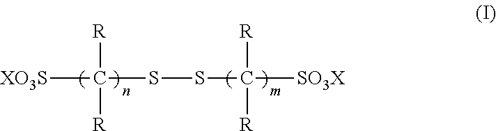
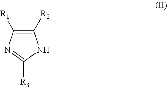
TABLE 1COMPONENTAMOUNTCopper sulfate pentahydrate220g / LSulfuric acid40g / LChloride ion from hydrochloric acid50ppmPolyethylene glycol2g / L4-phenylimidazole / imidazole / 1,4-butandiol50mg / Ldiglycidyl ether copolymerBis-sodium sulfopropyl)-disulfide10mg / L

[0031]The coupon was connected to a conventional DC rectifier. The counter electrode in each plating cell was an insoluble. The plating bath ...

example 2

Comparative

[0033]Three FR4 / glass-epoxy coupons 5 cm wide, 15 cm long and 100 μm thick with a plurality of through-holes were provided by Tech Circuit. The through-holes had an average diameter of 100 μm. The coupons were processed through electroless copper using CIRCUPOSIT™ 880 Electroless Process plating formulations and method. The thickness of the electroless copper layer on each coupon was 0.3 μm. Each coupon was cleaned and electroplated with a flash copper layer 5 μm thick as described in Example 1 above. Each coupon was then placed in a dessicator during the interim before further processing to discourage any oxide formation on the copper.

[0034]Upon removal of the coupons from the dessicator, they were cleaned using a conventional copper cleaner to remove any possible oxide layer and have a clean copper surface for plating. Each coupon was then placed into separate plating cells with a fresh copper electroplating bath having the formulation in Table 1. The plating baths were...

example 3

[0035]Three FR4 / glass-epoxy coupons 5 cm wide, 15 cm long and 100 μm thick with a plurality of through-holes were provided by Tech Circuit. The through-holes had an average diameter of 100 μm. The coupons had a layer of electroless copper 0.3 μm thick. Each coupon was cleaned and electroplated with a flash copper layer 5 μm thick as described in Example 1 above. The coupons were stored in a dessicator prior to further treatment and plating.

[0036]Upon removal from storage, the flashed coupons were cleaned to remove any oxide layer and have a clean copper surface for plating. After cleaning, one coupon was transferred to a plating bath having the formula of Table 1. The second coupon was first immersed in an aqueous solution of 5.5 ppm bis(3-sulfopropyl)disulfide, sodium salt (SPS) and 10 wt % sulfuric acid for two minutes and then transferred into the copper electroplating bath. Copper electroplating was done at a current density of 1.5 A / dm2 with continuous air agitation of the bath...


PUM

PropertyMeasurementUnit
diametersaaaaaaaaaa
thicknessaaaaaaaaaa
thickaaaaaaaaaa

Abstract

The methods inhibit or reduce dimpling and voids during copper electroplating of through-holes with flash copper layers in substrates such as printed circuit boards. An acid solution containing disulfide compounds is applied to the through-holes of the substrate followed by filling the through-holes with copper using an acid copper electroplating bath which includes additives such as brighteners and levelers.

Description

FIELD OF THE INVENTION[0001]The present invention is directed to a method of filling through-holes having a layer of flash copper which reduces or inhibits the formation of dimples and voids. More specifically, the present invention is directed to a method of filling through-holes having a layer of flash copper which reduces or inhibits the formation of dimples and voids by applying an aqueous acid pretreatment solution containing disulfide compounds at low concentrations to the through-holes with the flash copper layer followed by filling the through-holes with copper using an acid copper electroplating bath containing brighteners and levelers.BACKGROUND OF THE INVENTION[0002]High density interconnects is an important design in the fabrication of printed circuit boards with microvias and through-holes. Miniaturization of these devices relies on a combination of thinner core materials, reduced line widths and smaller diameter through-holes and blind vias. The diameters of the throug...

Claims


Application Information

Patent Timeline
Patent Type & Authority Applications(United States)
IPC IPC(8): C25D5/02
CPCC25D3/38C25D5/10C25D5/02C23C18/1653H05K3/425C25D5/34H05K3/423
Inventor JAYARAJU, NAGARAJANNAJJAR, ELIE H.BARSTAD, LEON R.
Owner ROHM & HAAS ELECTRONICS MATERIALS LLC
Why Eureka
Try Eureka