Stacked Integrated Circuit System

a technology of integrated circuits and stacks, applied in semiconductor devices, semiconductor/solid-state device details, instruments, etc., can solve the problems of wasting a lot of layout space, bringing some problems into integrated circuits, and their gigantic size (hundred times bigger)

Inactive Publication Date: 2014-09-18
IPENVAL CONSULTANT
View PDF7 Cites 21 Cited by
  • Summary
  • Abstract
  • Description
  • Claims
  • Application Information

AI Technical Summary

Benefits of technology

[0004]In one embodiment of the present invention, a stacked integrated circuit system is provided to comprise a first chip with first average pattern density comprising memory cells, a second chip with second average pattern density comprising logic circuitries for the memory cells and a functioning unit and a plurality of through-silicon vias within one of the first chip and second chip to electrically connect the first chip and the second chip, wherein the memory cells of the first chip and the logic circuitries of the second chip are designed to be used collectively in order to perform complete memory functions, and wherein the first average pattern density is higher than the second average pattern density.

Problems solved by technology

Although through-silicon vias come with many advantages, they also bring some issues into integrated circuits.
For example, their gigantic size (hundred times bigger than traditional transistors) compared to their neighbors such as transistors, interconnections etc. would waste a lot of layout space.
The more space they waste, the bigger a chip will be.
Nowadays, all the electronic devices are expected to be small so wasting space is definitely not a smart idea.

Method used


Image

  • Stacked Integrated Circuit System
  • Stacked Integrated Circuit System
  • Stacked Integrated Circuit System

Examples


Embodiment Construction

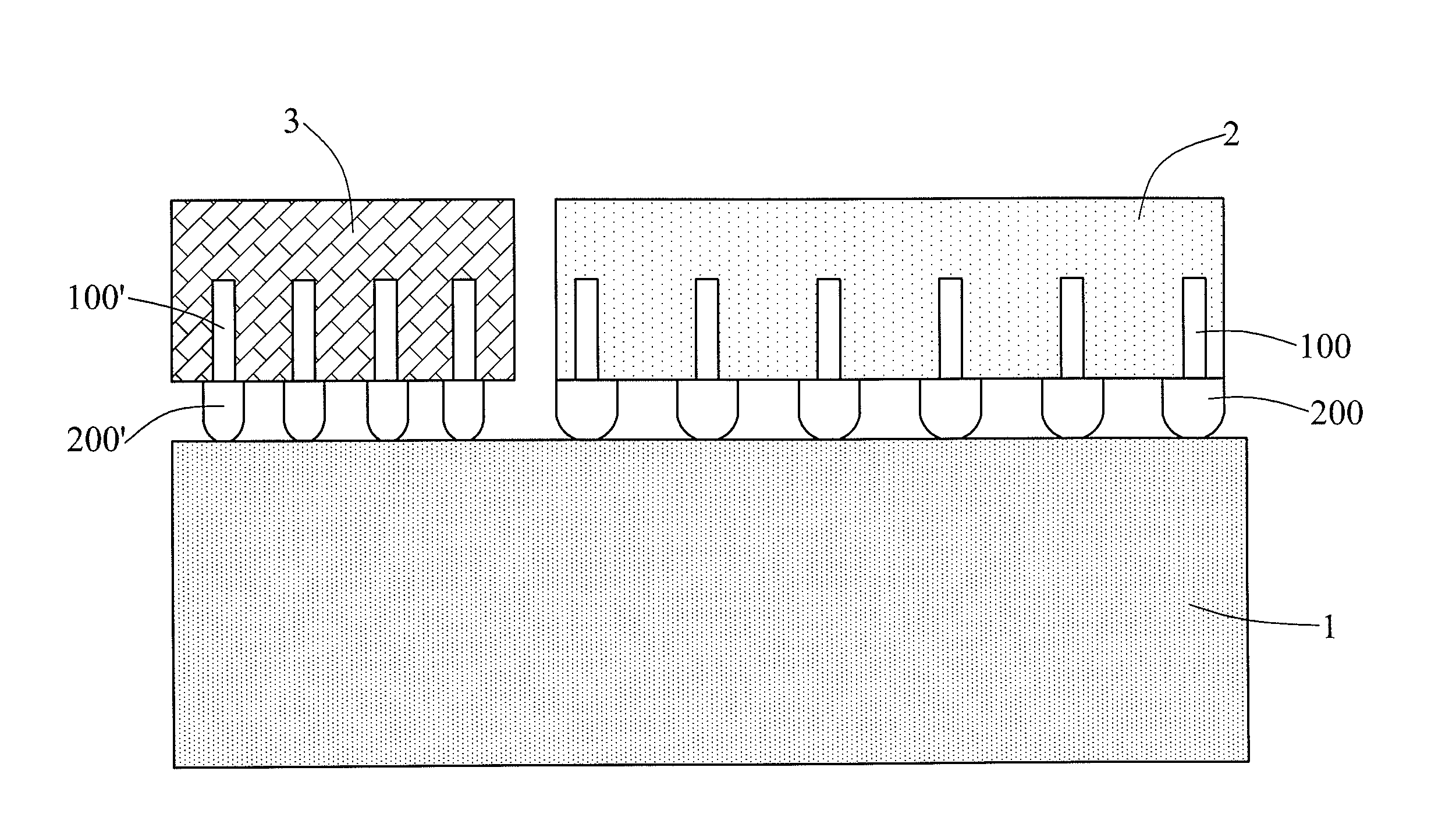
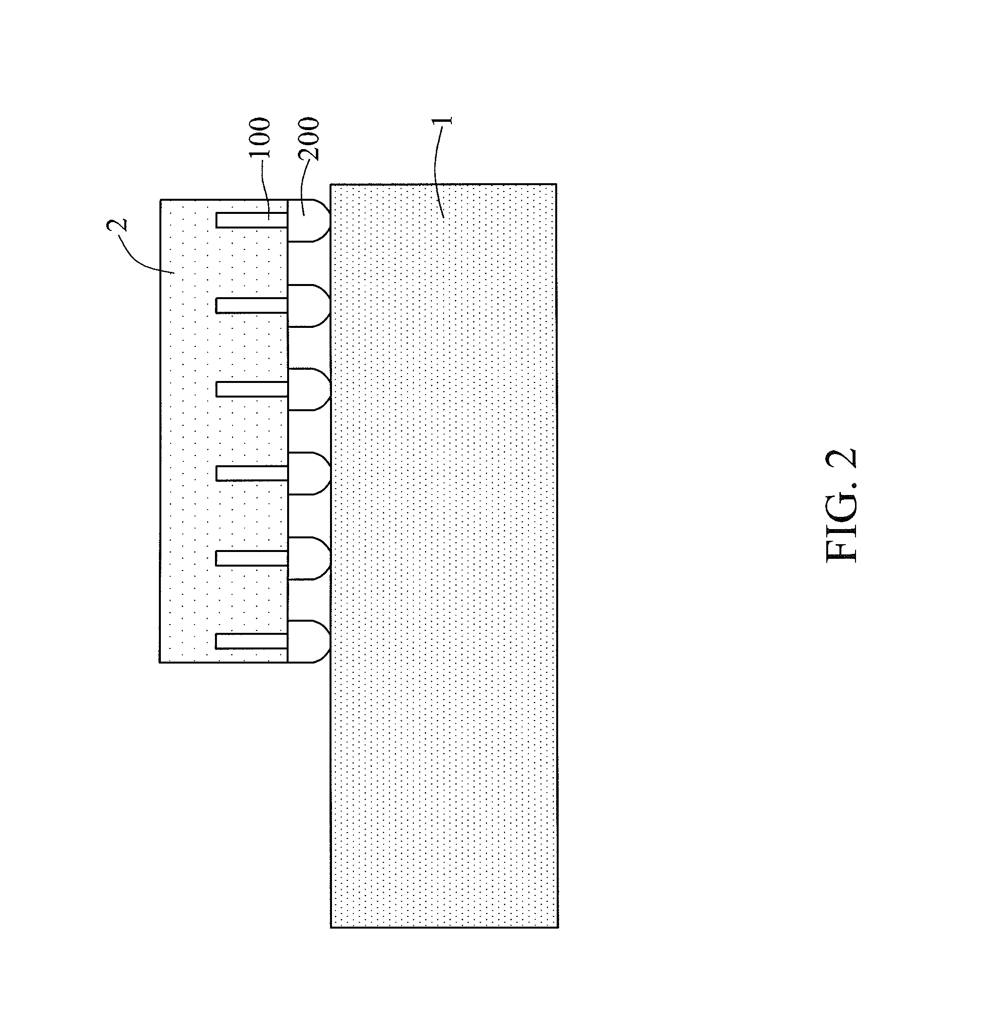
[0015]The following is the detailed description of the preferred embodiments of this invention. All the elements, sub-elements, structures, materials, arrangements recited herein can be combined in any way and in any order into new embodiments, and these new embodiments should fall in the scope of this invention defined by the appended claims. A person skilled in the art, upon reading this invention, should be able to modify and change the elements, sub-elements, structures, materials, arrangements recited herein without being apart from the principle and spirit of this invention. Therefore, these modifications and changes should fall in the scope of this invention defined only by the following claims.

[0016]There are a lot of embodiments and figures in this application. To avoid confusions, similar components are represented by same or similar numerals. To avoid complexity and confusions, only one of the repetitive components is marked. Figures are meant to deliver the principle and...


PUM


Abstract

A stacked integrated circuit system comprises a first chip with first average pattern density comprising memory cells, a second chip with second average pattern density comprising logic circuitries for the memory cells and a functioning unit and a plurality of through-silicon vias within one of the first chip and second chip to electrically connect the first chip and the second chip, wherein the memory cells of the first chip and the logic circuitries of the second chip are designed to be used collectively in order to perform complete memory functions, and wherein the first average pattern density is higher than the second average pattern density.

Description

FIELD OF THE INVENTION[0001]The present invention relates to a stacked integrated circuit system and particularly to a stacked integrated circuit system using through-silicon vias.BACKGROUND OF THE INVENTION[0002]To save precious layout space or increase interconnection efficiency, multiple chips of integrated circuits (ICs) can be stacked together as a single IC package. To that end, a three-dimensional (3D) stack packaging technology is used to package the chips of integrated circuits. Through-silicon vias (TSVs) are widely used to accomplish the 3D stack packaging technology. A through-silicon via is a vertical conductive via completely passing through a silicon wafer, a silicon board, a substrate of any material or die. Nowadays, a 3D integrated circuit (3D IC) is applied to a lot of fields such as memory stacks, image sensors or the like.[0003]Although through-silicon vias come with many advantages, they also bring some issues into integrated circuits. For example, their gigant...

Claims


Application Information

Patent Timeline
Patent Type & Authority Applications(United States)
IPC IPC(8): H01L25/18
CPCH01L25/18H01L2224/16265H01L23/522H01L24/13H01L24/16H01L24/81H01L25/0657H01L2224/13025H01L2224/16145H01L2224/81191H01L2224/81193H01L2924/1431H01L2924/1436H01L2924/1437H01L2924/19104H01L2225/06513H01L2225/06541H01L2225/06568G11C5/025
Inventor HUANG, CHAO-YUANHO, YUEH-FENGYANG, MING-SHENGCHEN, HWI-HUANG
Owner IPENVAL CONSULTANT
Why Eureka
Try Eureka