MEMS Chip and Manufacturing Method Thereof

a technology of microelectromechanical systems and mems chips, applied in the direction of fluid speed measurement, instruments, coatings, etc., can solve the problems of limited design flexibility, difficult to integrate different types of mems devices in one mems chip, and inability to manufacture such a mems chip

Inactive Publication Date: 2015-07-30
RICHTEK TECH
View PDF2 Cites 6 Cited by
  • Summary
  • Abstract
  • Description
  • Claims
  • Application Information

AI Technical Summary

Benefits of technology

[0017]From another perspective, the present invention provides a MEMS chip, comprising: a cap layer, which includes a first substrate, wherein the first substrate has a first region and a second region, the first region having a plurality of first trenches formed therein, the second region having a plurality of second trenches formed therein, each of the first trenches and each of the second trenches having a same depth, a first etch pattern density of the first region being higher than a second etch pattern density of the second region; and a composite device layer, which includes a second substrate, and a first MEMS device and a second MEMS device on or above the second substrate; wherein the cap layer is bonded with the composite device layer such that, between the cap layer and the composite device layer, a first chamber and a second chamber are formed in correspondence to the locations of the first region and the second region, respectively, wherein the first chamber accommodates the first MEMS device and the second chamber accommodates the second MEMS device.

Problems solved by technology

This constraint significantly limits the design flexibility; for example, it is very difficult to integrate different types of MEMS devices in one MEMS chip.
However, the conventional WLP process can not manufacture such a MEMS chip.
However, in such prior art, it is required to form trenches of different depths by multiple etching steps, which requires complicated etch control and the manufacturing variance makes it more difficult to maintain consistent high accuracy.

Method used


Image

  • MEMS Chip and Manufacturing Method Thereof
  • MEMS Chip and Manufacturing Method Thereof
  • MEMS Chip and Manufacturing Method Thereof

Examples


first embodiment

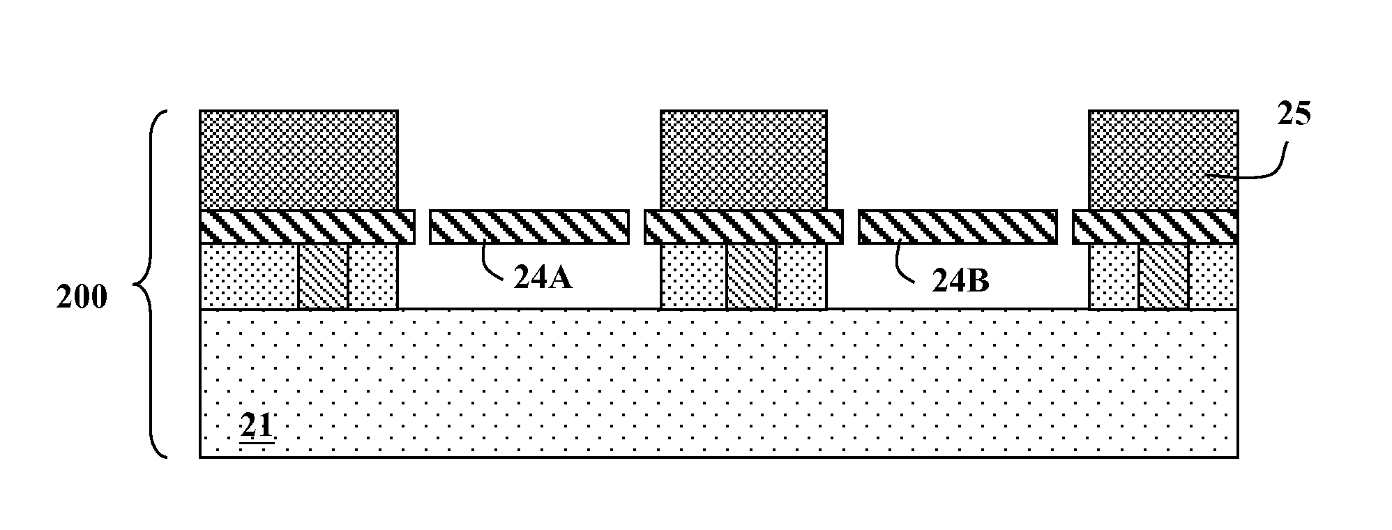
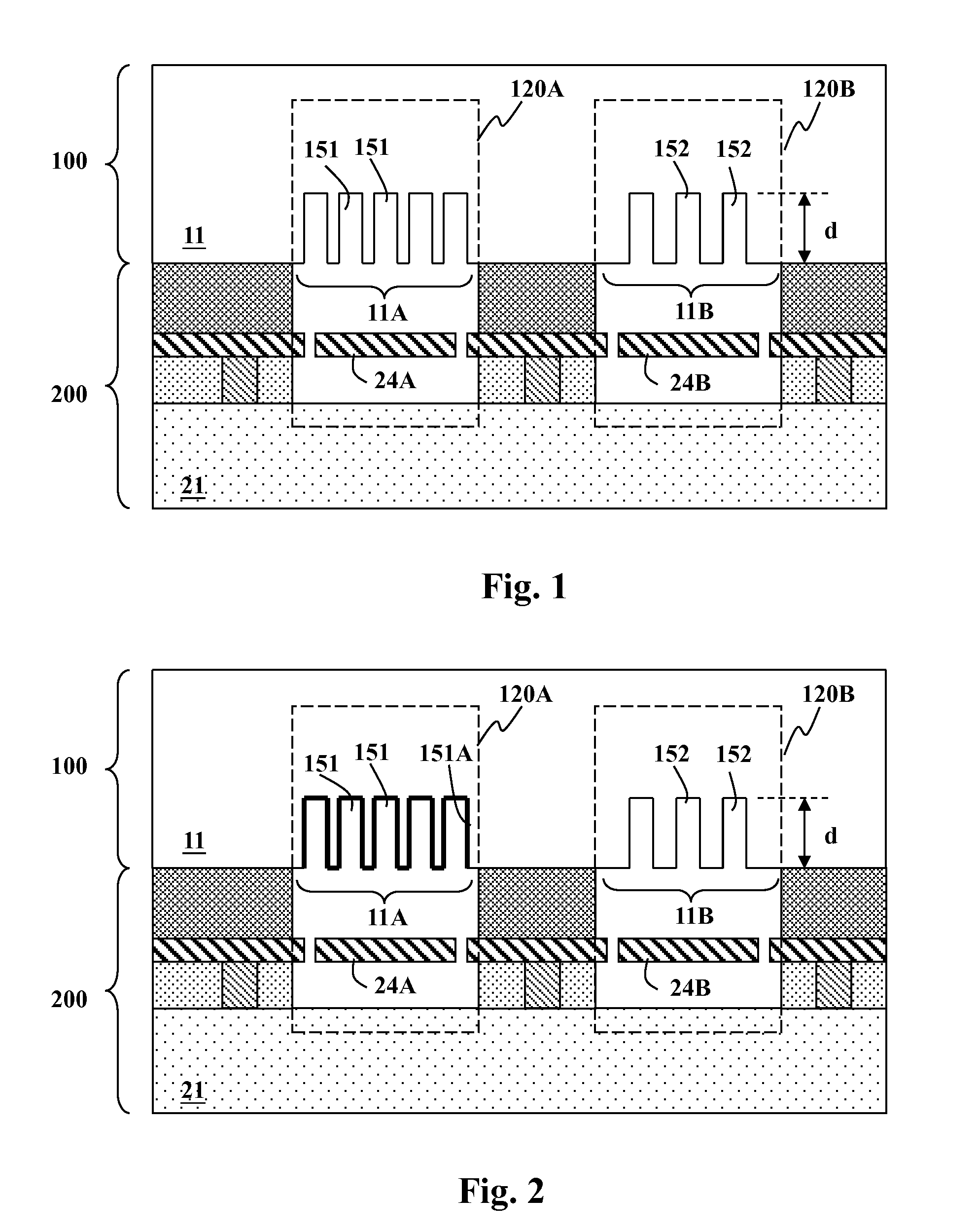
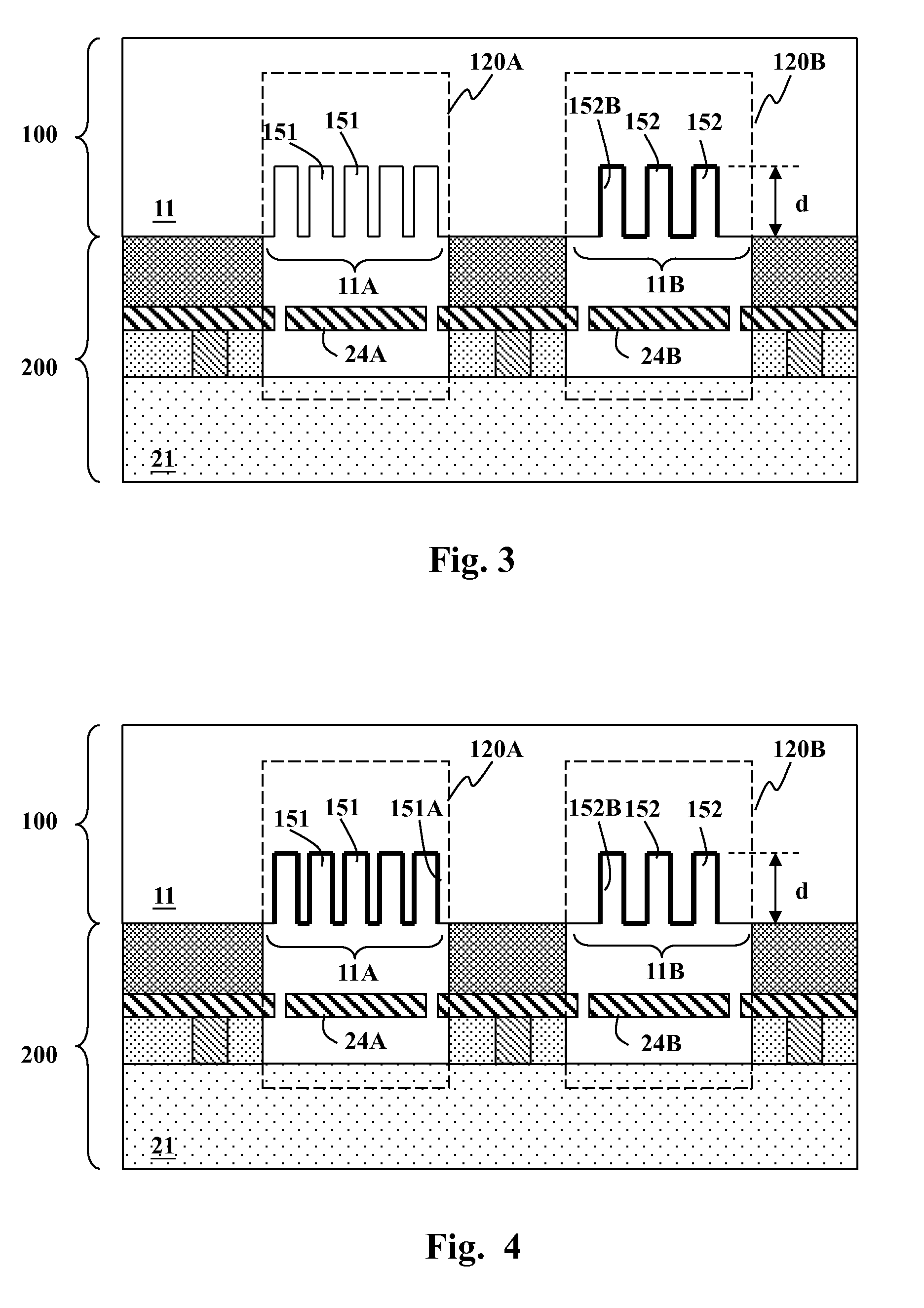
[0039]FIGS. 11-13 show schematic cross sectional views of a first embodiment for making the composite device wafer according to the present invention. First, a second substrate 21, e.g. silicon substrate, is provided, and next the desired patterns of multiple layers are manufactured on the second substrate 21 via a standard CMOS process. One of the layers is a sacrificial layer 22 surrounding the first MEMS device 24A and the second MEMS device 24B. A hard mask layer 23 can be included in the structure, located on or above the sacrificial layer 22. The material of the sacrificial layer 22 is different from the materials of the other parts of the structure (the first MEMS device 24A, the second MEMS device 24B, the material layer 25 and the material layer 26) surrounding the sacrificial layer 22. An appropriate etchant is provided to etch the sacrificial layer 22 and such appropriate etchant should have an appropriate etch selectivity to the above-mentioned surrounding parts (the fir...

second embodiment

[0042]FIGS. 14-16 show schematic cross sectional views of a second embodiment for making the composite device wafer according to the present invention. In this embodiment, the composite device wafer 200 is formed by bonding a CMOS wafer 200A to a MEMS wafer 200B (as shown in FIGS. 14-15). In the MEMS wafer 200B, the structure and layout of the first MEMS device 24A and the second MEMS device 24B have already been defined and formed. The CMOS wafer 200A includes a second substrate 21 (e.g., silicon substrate) and a microelectronic circuit (not shown), manufactured by a standard CMOS process. In this embodiment, because it is required to electronically connect the microelectronic circuit of the CMOS wafer 200A to the first MEMS device 24A and the second MEMS device 24B of the MEMS wafer 200B, plural conductive plugs 28 are preferably provided. Next, the CMOS wafer 200A is bonded to the MEMS wafer 200B by providing a conducting adhesive in between, or by providing any adhesive which do...


PUM

PropertyMeasurementUnit
pressureaaaaaaaaaa
pressureaaaaaaaaaa
etch pattern densityaaaaaaaaaa

Abstract

A MEMS chip includes a cap layer and a composite device layer. The cap layer includes a substrate. The substrate has a first region and a second region, wherein the first region includes plural first trenches and the second region has plural second trenches. The first region has a first etch pattern density and the second region has a second etch pattern density, wherein the first etch pattern density is higher than the second etch pattern density to form chambers of different pressures.

Description

CROSS REFERENCE[0001]The present invention claims priority to TW 103102894, filed on Jan. 27, 2014.BACKGROUND OF THE INVENTION[0002]1. Field of Invention[0003]The present invention relates to a micro-electro-mechanical-system (MEMS) chip and a manufacturing method thereof; particularly, it relates to such MEMS chip and manufacturing method thereof wherein different regions of a cap wafer have different etch pattern densities, such that the MEMS chip has different chambers of different pressures.[0004]2. Description of Related Art[0005]In making a MEMS chip, it is often required to package a MEMS device such as a micro-acoustical sensor, gyro-sensor or accelerometer, etc. in a sealed space. Different types of MEMS devices require different operation pressures in the sealed space. For example, a gyro-sensor usually operates under 0.1 mbar to 10 mbar, whereas an accelerometer usually operates under 200 mbar to 1000 mbar. In a typical Wafer Level Packaging (WLP) method, only one operati...

Claims


Application Information

Patent Timeline
Patent Type & Authority Applications(United States)
IPC IPC(8): B81C1/00B81B7/00
CPCB81C1/00269B81C1/00238B81C1/00595B81B7/0038B81B7/02B81B2207/015B81C2201/019B81C1/00285B81C2201/013B81C2203/0792
Inventor KANG, YU-FULO, CHIUNG-CHENG
Owner RICHTEK TECH
Why Eureka
Try Eureka