Method of manufacturing semiconductor device

Inactive Publication Date: 2009-03-12
SK HYNIX INC
View PDF4 Cites 11 Cited by
  • Summary
  • Abstract
  • Description
  • Claims
  • Application Information

AI Technical Summary

Benefits of technology

[0008]The invention provides a method of manufacturing a semiconductor device in which when the gate etching process is performed, the etching-obstructing layer is formed on an interface of the conductive layer on an area having a low density metal layer pattern and the metal layer remaining on an area having a high density metal layer pattern so as to change an etching selection ra

Problems solved by technology

However, there are problems that if a thickness of the layer to be etched is small, the tungsten silicide layer between the predetermined areas for forming the word lines remains and if a thickness of the layer to be etched is large, the dielectric layer between the predetermined areas for forming the select line is attacked.
In addition, in a case where, after an over-etching process, the tungsten

Method used


Image

  • Method of manufacturing semiconductor device
  • Method of manufacturing semiconductor device
  • Method of manufacturing semiconductor device

Examples


Embodiment Construction

[0023]Hereinafter, the preferred embodiments of the invention are explained in more detail with reference to the accompanying drawings. However, the embodiments of the invention may be modified in various ways and the scope of the invention is not to be limited to the illustrated embodiment. The description herein is provided for illustrating more completely to those skilled in the art.

[0024]The invention is not limited to a process of manufacturing a NAND flash memory, but is applicable to technology for manufacturing semiconductor devices such as dynamic random access memory (DRAM) and the static random access memory (SRAM). In the following description, the NAND flash memory device is illustrated as one example.

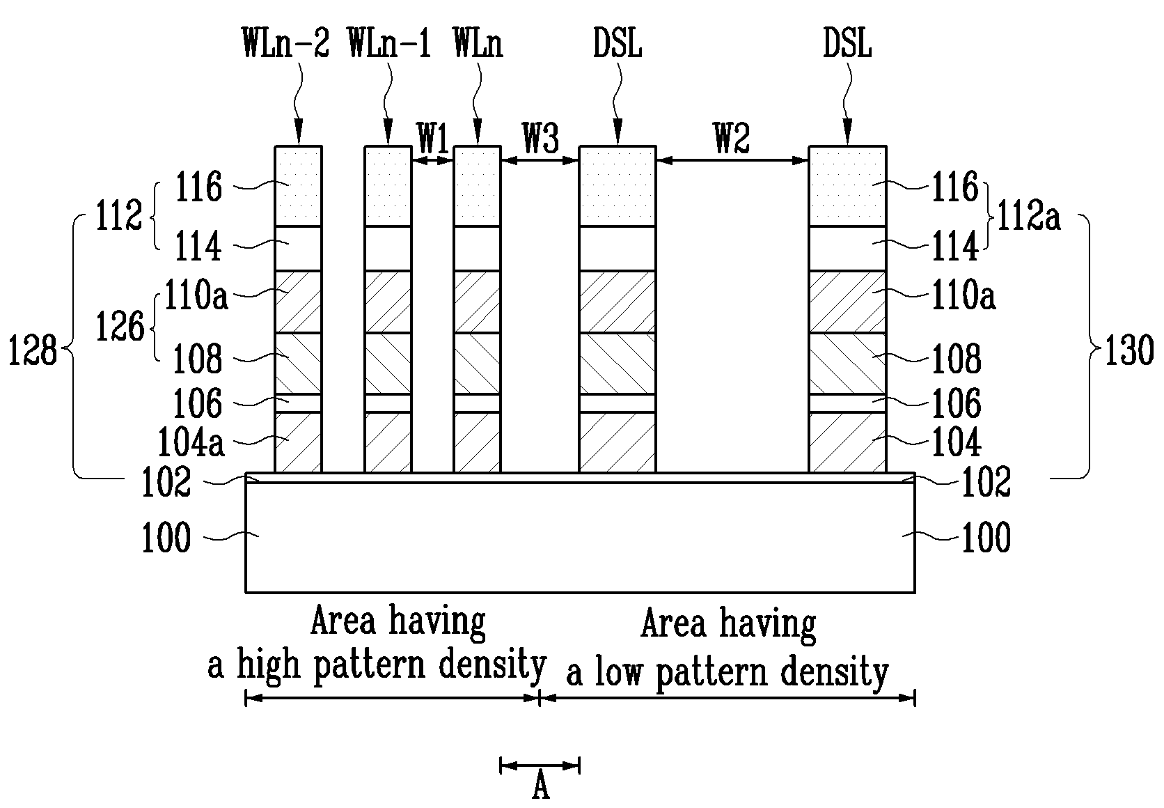
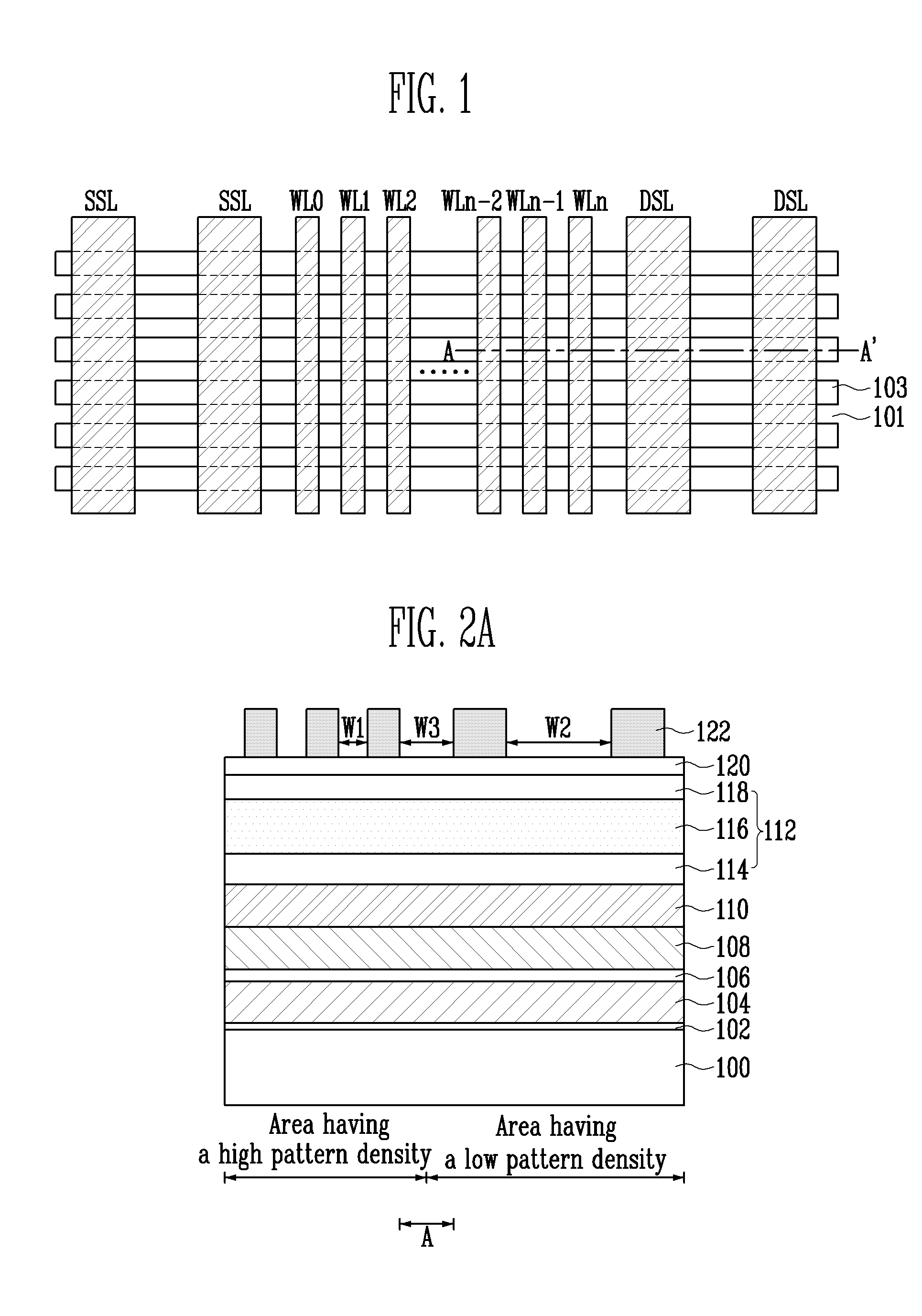
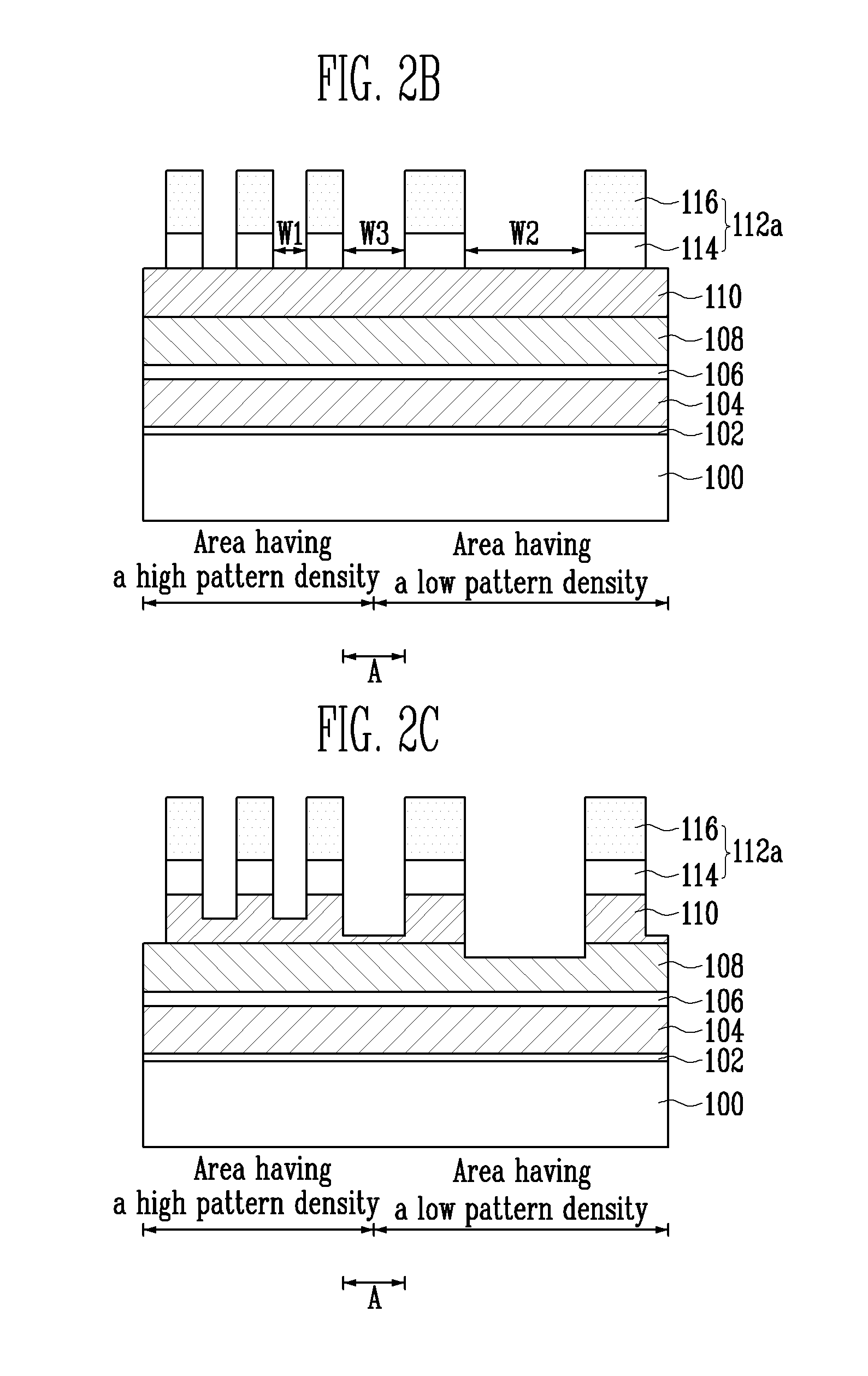
[0025]FIG. 1 is a layout of a flash memory device according to one embodiment of the invention and FIG. 2A to FIG. 2F are sectional views taken along the line A-A′ in FIG. 1 and showing a process for manufacturing the flash memory device of FIG. 1.

[0026]Referring to FIG. 1...


PUM


Abstract

A method of manufacturing a semiconductor device comprising forming a conductive layer on a semiconductor substrate; forming a metal layer on the conductive layer; performing a first etching process for patterning the metal layer on a first area to form first metal layer patterns at relatively wide intervals until the conductive layer of the first area is exposed; performing a second etching process for forming an etching-obstructing layer on the first area and patterning the metal layer on a second area to form second metal layer patterns at relatively narrow intervals until the conductive layer of the second area is exposed; removing the etching-obstructing layer; and removing an exposed area of the conductive layer to form a conductive pattern.

Description

CROSS-REFERENCE TO RELATED APPLICATION[0001]The priority of Korean Patent Application No. 2007-0090294, filed on Sep. 6, 2007, the disclosure of which is incorporated herein by reference in its entirety, is claimed.BACKGROUND OF THE INVENTION[0002]The invention relates to a method of manufacturing a semiconductor device and, more particularly, relates to a method of manufacturing a semiconductor device which can improve a loading effect according to a pattern density during a gate etching process.[0003]In a flash memory device, data are stored through a program operation in which electrons are injected to a floating gate through Fowler-Nordheim (F-N) tunneling or an erase operation in which electrons are discharged from the floating gate through F-N tunneling. In such flash memory device, a drain select line, a source select line, and a plurality word lines crossing an isolation layer are formed, each of the word lines being disposed between the drain select line and the source sele...

Claims


Application Information

Patent Timeline
IPC IPC(8): H01L21/441
CPCH01L21/32137H01L21/28061H01L21/28052H01L21/67069
Inventor LEE, IN NO
Owner SK HYNIX INC
Why Eureka
Try Eureka