Method of nano-patterning using surface plasmon effect and method of manufacturing nano-imprint master and discrete track magnetic recording media using the nano-patterning method

Active Publication Date: 2009-04-02
SAMSUNG ELECTRONICS CO LTD
View PDF2 Cites 20 Cited by
  • Summary
  • Abstract
  • Description
  • Claims
  • Application Information

AI Technical Summary

Benefits of technology

[0010]To address the above and/or other problems, exemplary embodiments of the present invention provides a method of nano-patterning that can realize a minute line width and high pa

Problems solved by technology

A related art photolithography method is limited in its ability to manufacture the minute pattern, and thus, many studies have been conducted to use an electron beam lithography method and a nano-imprinting method in manufacturing the minute patterns.
While the method of manufacturing a minute pattern using electron beam lithography described above has an advantage

Method used


Image

  • Method of nano-patterning using surface plasmon effect and method of manufacturing nano-imprint master and discrete track magnetic recording media using the nano-patterning method
  • Method of nano-patterning using surface plasmon effect and method of manufacturing nano-imprint master and discrete track magnetic recording media using the nano-patterning method
  • Method of nano-patterning using surface plasmon effect and method of manufacturing nano-imprint master and discrete track magnetic recording media using the nano-patterning method

Examples


Embodiment Construction

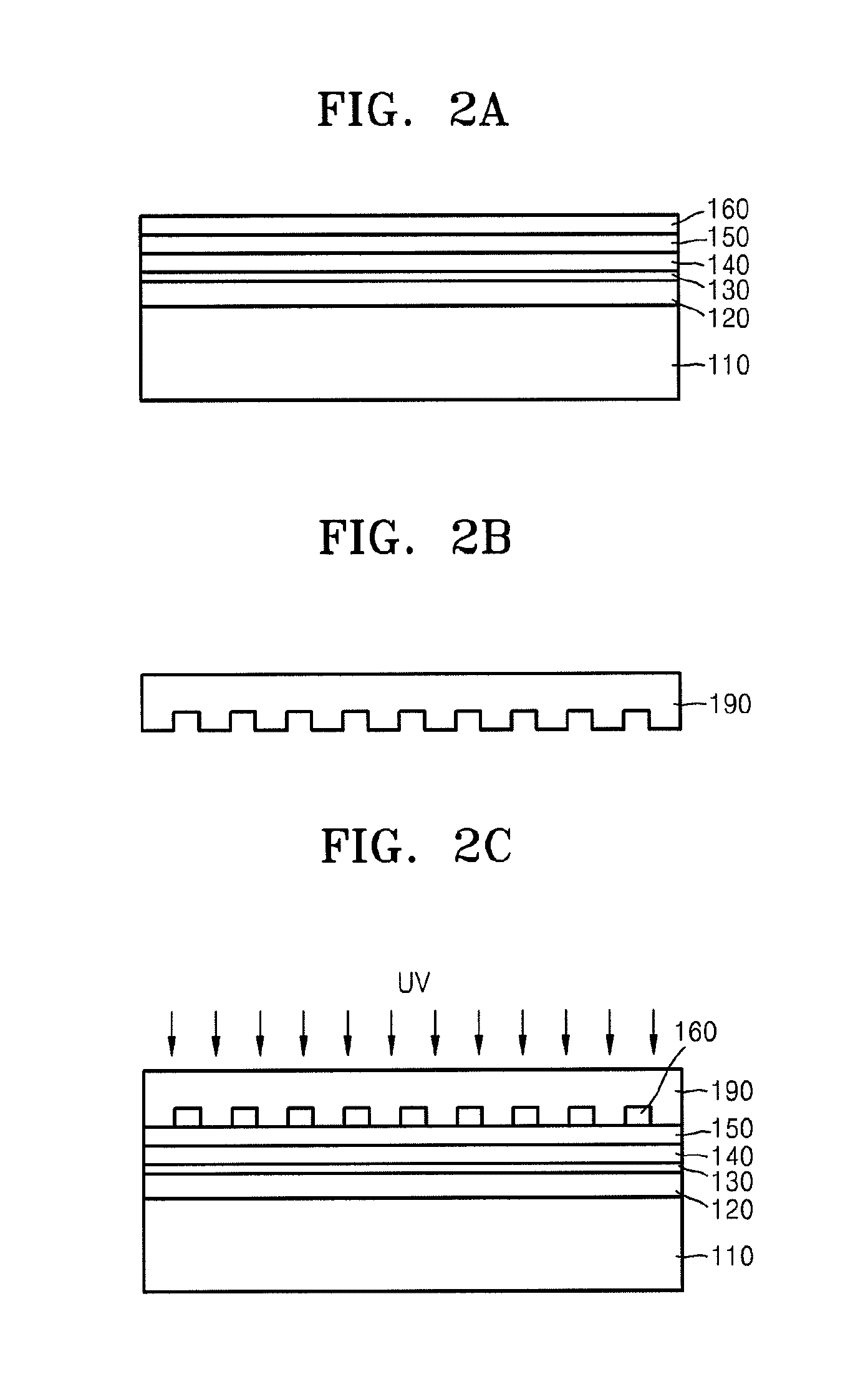
[0020]The present invention will now be described more fully with reference to the accompanying drawings in which exemplary embodiments of the invention are shown. In the drawings, the thicknesses of layers and regions are exaggerated for clarity, and like reference numerals refer to like elements.

[0021]FIGS. 2A through 2K are cross-sectional views for explaining a method of nano-patterning according to an exemplary embodiment of the present invention. Referring to FIG. 2A, an etching object material layer 120, a photoresist layer 140, a metal layer 150, and a polymer layer 160 are formed on a substrate 110. An antireflection film 130, such as a bottom antireflective coating (BARC) for preventing the photoresist layer 140 from being re-exposed to light reflected by the substrate 110 when the light is radiated during an exposure process, can further be formed between the etching object material layer 120 and the photoresist layer 140. The metal layer 150 is formed to expose the photo...


PUM

PropertyMeasurementUnit
Densityaaaaaaaaaa
Radiusaaaaaaaaaa
Wavelengthaaaaaaaaaa

Abstract

A method of nano-patterning, a method of manufacturing a nano-imprinting master and a discrete track magnetic recording medium are all provided. The method of nano-patterning includes (a) sequentially forming on a substrate an etching object material layer, a photoresist layer, and a metal layer patterned to a first pattern having a structure in which line patterns are repeatedly arranged with a predetermined interval; (b) irradiating light onto a surface of the metal layer to excite surface plasmon so that the photoresist layer is exposed to a second pattern by the surface plasmon; (c) removing the metal layer and developing the photoresist layer; and (d) etching the etching object material layer using the photoresist layer patterned to the second pattern as a mask.

Description

CROSS-REFERENCE TO RELATED PATENT APPLICATIONS[0001]This application claims priority from Korean Patent Application No. 10-2007-0098901, filed on Oct. 1, 2007, in the Korean Intellectual Property Office, the disclosure of which is incorporated herein in its entirety by reference.BACKGROUND OF THE INVENTION[0002]1. Field of the Invention[0003]The present invention relates to a method of nano-patterning that realizes a high pattern density using a surface plasmon effect and a method of manufacturing a nano-imprinting master that can copy a nano-pattern and a discrete track magnetic recording medium for high density magnetic recording using the nano-patterning method.[0004]2. Description of the Related Art[0005]Recently, a method of nano-patterning that can realize a minute line width has received much attention. For example, in a semiconductor apparatus, a further increase in the number of devices per unit area is required in order to achieve a high integration density, and for this p...

Claims


Application Information

Patent Timeline
IPC IPC(8): G03F7/20B29C59/02B82B3/00B82Y10/00B82Y40/00G11B5/855H01L21/027
CPCG03F1/14G03F7/70375G03F7/2014G03F1/50B82Y40/00G03F7/0002G03F7/0015H01J37/3174H01L21/0273
Inventor KIM, HAE-SUNGLEE, MYUNG-BOKSOHN, JIN-SEUNG
Owner SAMSUNG ELECTRONICS CO LTD
Why Eureka
Try Eureka