Electronic component

a technology of electronic components and components, applied in the field of electronic components, can solve the problems of small mechanical distortion occurring upon application of voltage, audible sound, acoustic noise, and may occur achieve the effects of significantly reducing or preventing the occurrence of acoustic noise in the circuit board, reducing the amplitude of vibration, and reducing or preventing the occurrence of acoustic nois

Active Publication Date: 2014-09-18
MURATA MFG CO LTD
View PDF4 Cites 18 Cited by
  • Summary
  • Abstract
  • Description
  • Claims
  • Application Information

AI Technical Summary

Benefits of technology

[0025]With this configuration, if a joining material such as solder is supplied in an excessive amount, an amount of the joining material wetting and spreading on the end surfaces of the external electrodes of the laminated capacitor is significantly reduced, to significantly reduce or prevent the occurrence of acoustic noise.
[0026]When the laminated capacitor is mounted on the circuit board by utilizing the configuration of the electronic component according to a preferred embodiment of the present invention, the viscoelastic resin located in the space between the laminated capacitor and the substrate-type terminal absorbs at least part of the vibration that occurs in the laminated capacitor to reduce the amplitude of vibration transmitted to the circuit board, thus significantly reducing or preventing the occurrence of acoustic noise in the circuit board.

Problems solved by technology

In such a laminated capacitor, small mechanical distortion occurs upon application of voltage.
When this distortion is transmitted to the circuit board, audible sound, or as is commonly referred to as acoustic noise, may occur in the circuit board.
As such, external electrodes on a laminated capacitor and mounted electrodes on a circuit board are arranged in directions intersecting with each other, resulting in difficulty in transmitting the distortion in the laminated capacitor to the circuit board.
This means that the land pattern needs to be altered, which is difficult to achieve in current circuit boards of which high-density mounting is required.
Accordingly, the use of an interposer substrate having the above configuration results in difficulty in reducing the sizes of the circuit board and the like, thus contributing to increased costs.
However, since the recent increase in capacity of the laminated capacitor tends to increase the distortion in the laminated capacitor, the occurrence of acoustic noise in the circuit board is not sufficiently suppressed even if this configuration is adopted.

Method used


Image

  • Electronic component
  • Electronic component
  • Electronic component

Examples


first preferred embodiment

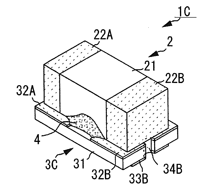
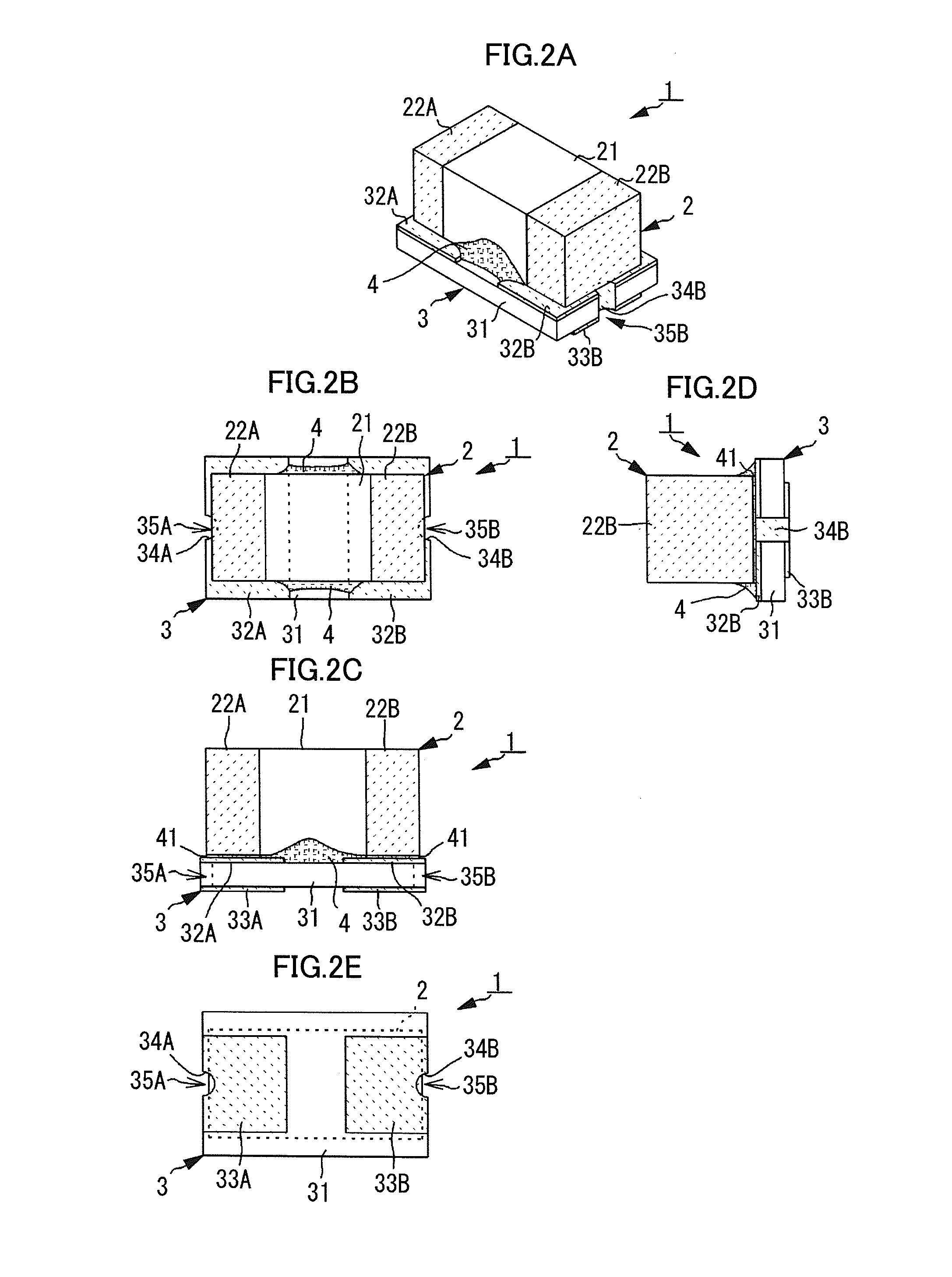
[0034]An electronic component 1 according to a first preferred embodiment of the present invention will be described below.

[0035]Electronic component 1 includes a laminated capacitor 2 described later, and a substrate-type terminal 3 described later. Examples of the laminated capacitor include a laminated ceramic capacitor including ceramic as a dielectric material, and a laminated metallized film capacitor including a resin film as a dielectric material. A laminated ceramic capacitor will be described herein by way of example.

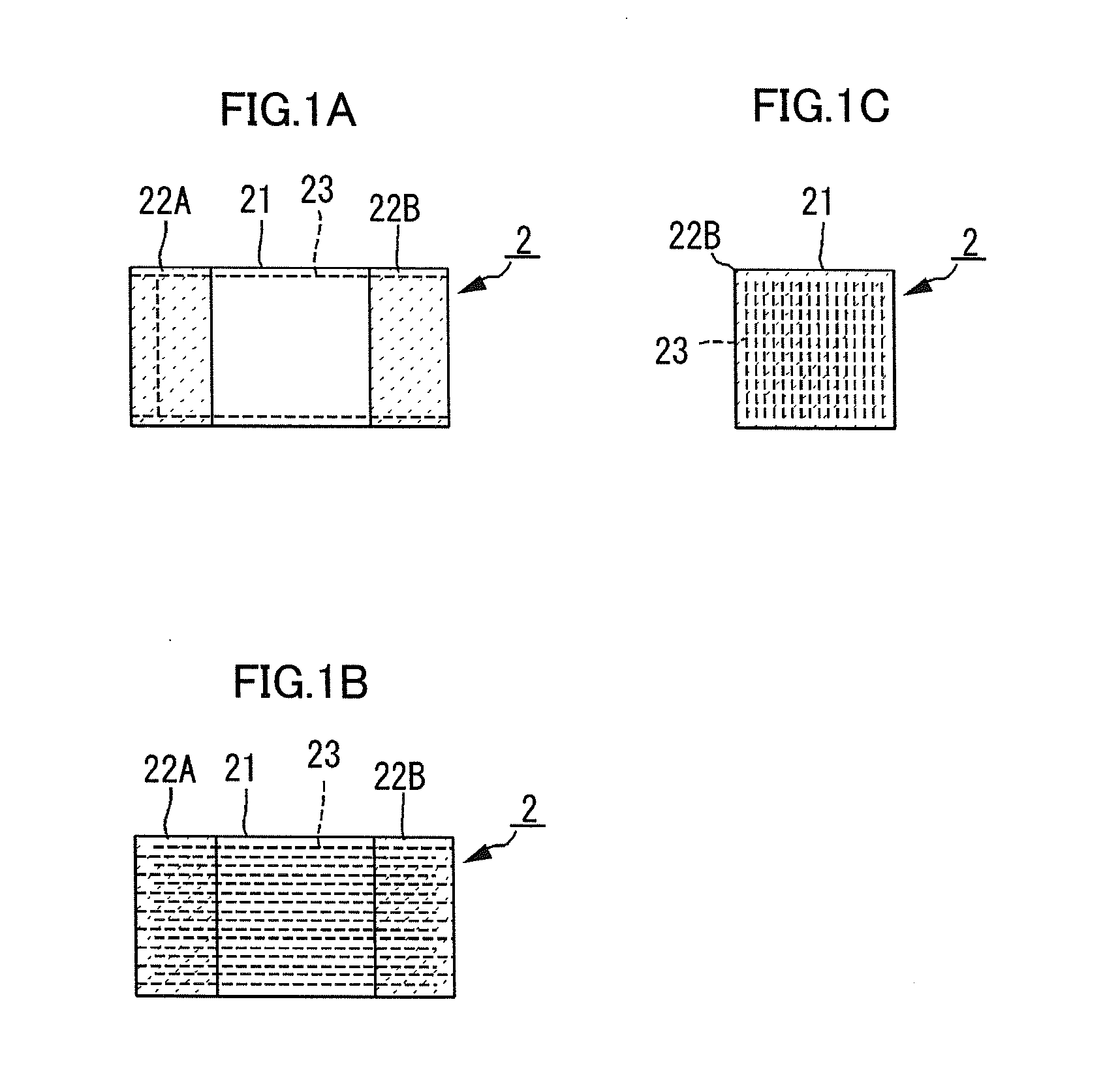
[0036]FIGS. 1A to 1C are a plan view, a front view and a right-side view of laminated capacitor 2, respectively.

[0037]Laminated capacitor 2 includes a laminated body 21, external electrodes 22A and 22B, and internal electrodes 23. Laminated body 21 preferably has a rectangular or substantially rectangular parallelepiped shape, with a first end surface (left-side surface) and a second end surface (right-side surface) located opposite to each other in a longitud...

second preferred embodiment

[0060]FIGS. 4A to 4D are a plan view, a front view, a right-side view and a bottom view, respectively, of an electronic component 1A according to a second preferred embodiment of the present invention.

[0061]Electronic component 1A in this preferred embodiment is the same as electronic component 1 in the first preferred embodiment in structure of laminated capacitor 2, but is different in that a substrate-type terminal 3A of a different size is provided. In the following description, therefore, the elements corresponding to those in the first preferred embodiment are designated by the same reference characters in the drawings and description thereof will not be repeated.

[0062]When viewed two-dimensionally, the outer shape of substrate-type terminal 3A is preferably the same as the outer shape of laminated capacitor 2 other than portions where grooves 35A and 35B are provided. As such, the entire arc-shaped or substantially arc-shaped portions of grooves 35A and 35B provided on the en...

third preferred embodiment

[0066]FIGS. 5A to 5C are a plan view, a front view and a right-side view of an electronic component 1B according to a third preferred embodiment of the present invention, respectively.

[0067]Electronic component 1B in this preferred embodiment is preferably the same as electronic component 1 in the first preferred embodiment in structure of laminated capacitor 2, but is different in that a substrate-type terminal 3B of a different size is provided. In the following description, therefore, the elements corresponding to those in the first preferred embodiment are designated by the same reference characters in the drawings and description thereof will not be repeated.

[0068]Substrate-type terminal 3B is provided with an area larger than the area of substrate-type terminal 3 shown in the first preferred embodiment. Grooves 35A and 35B provided on the end surfaces located in the longitudinal direction of substrate body 31 do not overlap with external electrodes 22A and 22B of laminated cap...


PUM


Abstract

An electronic component includes a laminated capacitor and a substrate-type terminal on which the laminated capacitor is mounted, with an viscoelastic resin located in a space between the laminated capacitor and the substrate-type terminal. The substrate-type terminal includes a substrate body, component connecting electrodes to mount the laminated capacitor are located on a component mounting surface of the substrate body, and external connecting electrodes to be connected to a circuit board are located on a substrate mounting surface of the substrate body.

Description

[0001]This non-provisional application is based on Japanese Patent Application No. 2013-052286 filed on Mar. 14, 2013 with the Japan Patent Office, the entire contents of which are hereby incorporated by reference.BACKGROUND OF THE INVENTION[0002]1. Field of the Invention[0003]The present invention relates to an electronic component including a laminated capacitor, and a substrate-type terminal having the laminated capacitor mounted thereon and mounted on a circuit board.[0004]2. Description of the Related Art[0005]Currently, chip components, and small laminated capacitors in particular, are frequently used on a circuit board of a mobile terminal such as a mobile telephone having an increasingly reduced thickness. A laminated capacitor includes a ceramic laminated body in a rectangular parallelepiped shape serving as a capacitor and including internal electrodes, and external electrodes formed on opposite end surfaces of the ceramic laminated body opposite to each other in a longitu...

Claims


Application Information

Patent Timeline
Patent Type & Authority Applications(United States)
IPC IPC(8): H01G4/30
CPCH01G4/308H01G2/02H01G4/224H01G4/228
Inventor HATTORI, KAZUOFUJIMOTO, ISAMU
Owner MURATA MFG CO LTD
Why Eureka
Try Eureka