Tungsten deposition sequence

a technology of tungsten and deposition sequence, applied in the direction of coating, chemical vapor deposition coating, metallic material coating process, etc., can solve the problems of void or seam, material gap, material gap, structural features on the device having decreased spatial dimensions, etc., to avoid tungsten “poisoning and enhance gapfilling

Inactive Publication Date: 2014-09-18
APPLIED MATERIALS INC
View PDF11 Cites 197 Cited by
  • Summary
  • Abstract
  • Description
  • Claims
  • Application Information

AI Technical Summary

Benefits of technology

[0007]Methods of filling gaps with tungsten are described. The methods include a tungsten dep-etch-dep sequence to enhance gapfilling yet avoid difficulty in restarting deposition after the intervening etch. The first tungsten deposition may have a nucleation layer or seeding layer to assist growth of the first tungsten deposition. Restarting deposition with a less-than-conductive nucleation layer would impact function of an integrated circuit, and therefore avoiding tungsten “poisoning” during the etch is desirable. The etching step may be performed using a plasma to excite a halogen-containing precursor while the substrate at relatively low temperature (near room temperature or less). The plasma may be local or remote. Another method may be used in combination or separately and involves the introduction of a source of oxygen into the plasma in combination with the halogen-containing precursor.

Problems solved by technology

The decreasing feature sizes result in structural features on the device having decreased spatial dimensions.
The widths of gaps and trenches on the device narrow to a point where the aspect ratio of gap depth to its width becomes high enough to make it challenging to fill the gap with material.
The depositing material is prone to clog at the top before the gap completely fills, producing a void or seam in the middle of the gap.

Method used


Image

  • Tungsten deposition sequence
  • Tungsten deposition sequence
  • Tungsten deposition sequence

Examples


Embodiment Construction

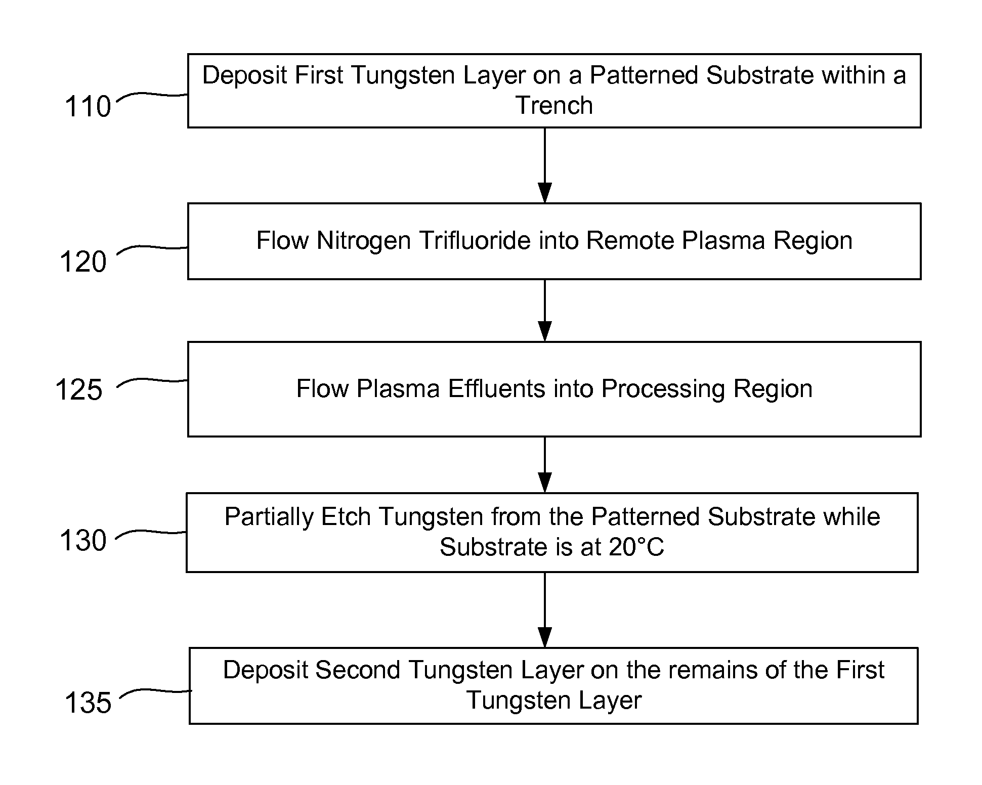
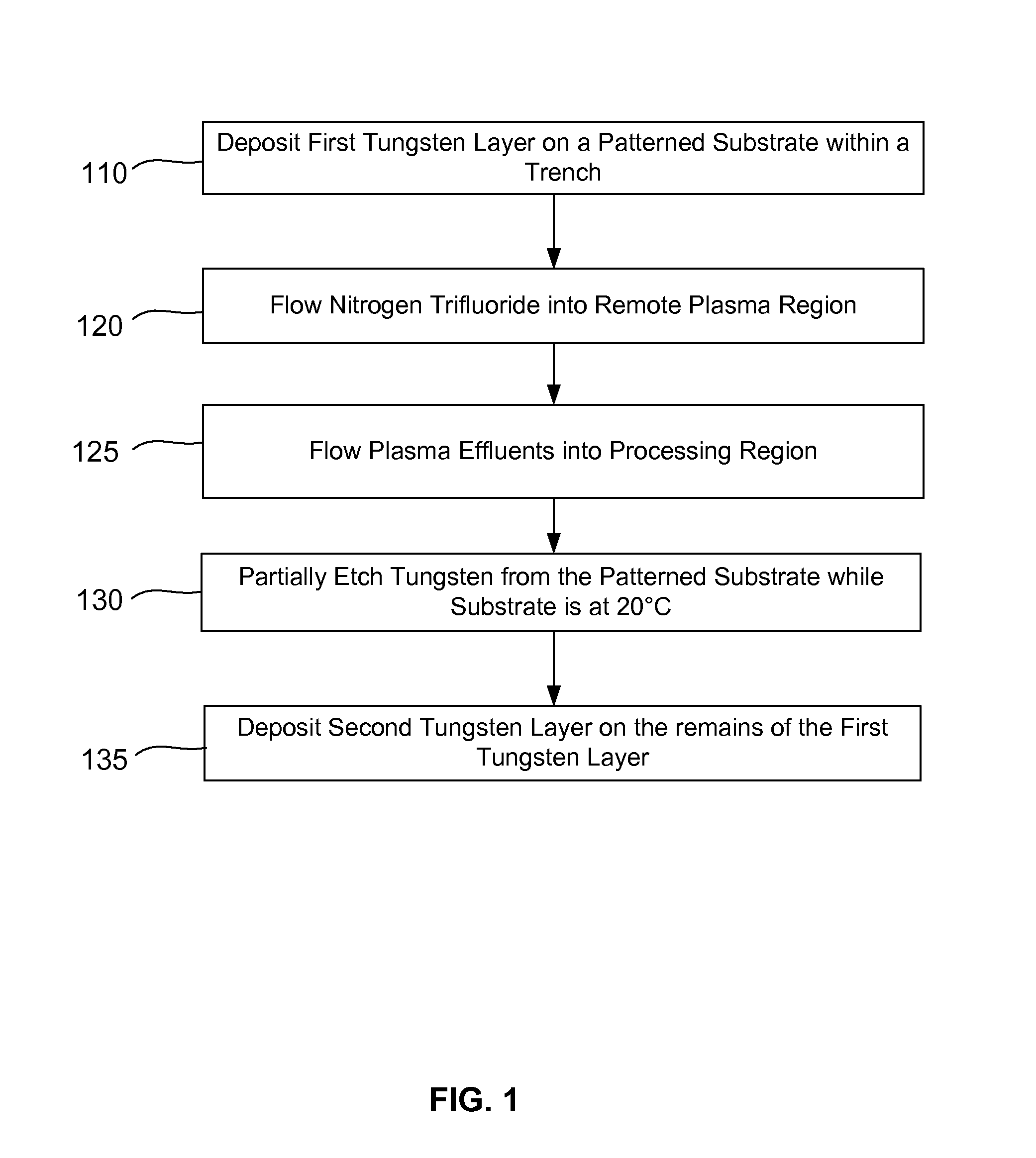
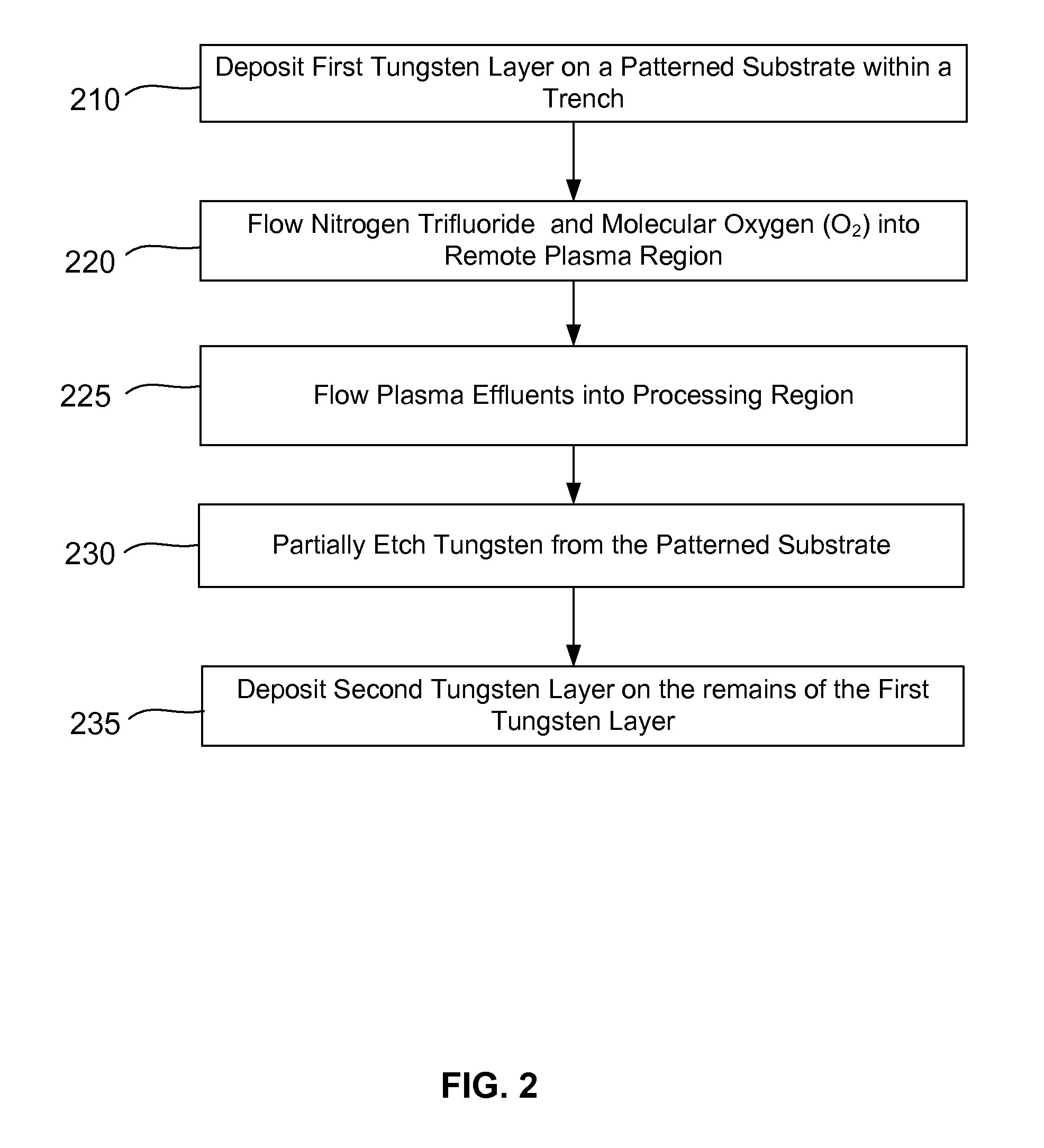
[0019]Methods of filling gaps with tungsten are described. The methods include a tungsten dep-etch-dep sequence to enhance gapfilling yet avoid difficulty in restarting deposition after the intervening etch. The first tungsten deposition may have a nucleation layer or seeding layer to assist growth of the first tungsten deposition. Restarting deposition with a less-than-conductive nucleation layer would impact function of an integrated circuit, and therefore avoiding tungsten “poisoning” during the etch is desirable. The etching step may be performed using a plasma to excite a halogen-containing precursor while the substrate at relatively low temperature (near room temperature or less). The plasma may be local or remote. Another method may be used in combination or separately and involves the introduction of a source of oxygen into the plasma in combination with the halogen-containing precursor.

[0020]The inventors have found new ways to deposit tungsten into trenches (e.g. contact h...


PUM

PropertyMeasurementUnit
temperatureaaaaaaaaaa

Abstract

Methods of filling gaps with tungsten are described. The methods include a tungsten dep-etch-dep sequence to enhance gapfilling yet avoid difficulty in restarting deposition after the intervening etch. The first tungsten deposition may have a nucleation layer or seeding layer to assist growth of the first tungsten deposition. Restarting deposition with a less-than-conductive nucleation layer would impact function of an integrated circuit, and therefore avoiding tungsten “poisoning” during the etch is desirable. The etching step may be performed using a plasma to excite a halogen-containing precursor while the substrate at relatively low temperature (near room temperature or less). The plasma may be local or remote. Another method may be used in combination or separately and involves the introduction of a source of oxygen into the plasma in combination with the halogen-containing precursor.

Description

CROSS-REFERENCES TO RELATED APPLICATIONS[0001]This application claims the benefit of U.S. Prov. Pat. App. No. 61 / 780,208 filed Mar. 13, 2013, and titled “TUNGSTEN DEPOSITION SEQUENCE,” which is hereby incorporated herein in its entirety by reference for all purposes.STATEMENT AS TO RIGHTS TO INVENTIONS MADE UNDER FEDERALLY SPONSORED RESEARCH AND DEVELOPMENT[0002]NOT APPLICABLEREFERENCE TO A “SEQUENCE LISTING,” A TABLE, OR A COMPUTER PROGRAM LISTING APPENDIX SUBMITTED ON A COMPACT DISK[0003]NOT APPLICABLEBACKGROUND OF THE INVENTION[0004]Semiconductor device geometries have dramatically decreased in size since their introduction several decades ago. Modern semiconductor fabrication equipment routinely produce devices with 32 nm, 28 nm, and 22 nm feature sizes, and new equipment is being developed and implemented to make devices with even smaller geometries. The decreasing feature sizes result in structural features on the device having decreased spatial dimensions. The widths of gaps ...

Claims


Application Information

Patent Timeline
Patent Type & Authority Applications(United States)
IPC IPC(8): H01L21/285
CPCH01L21/28562H01L21/76877C23C16/045C23C16/14C23C16/56H01L21/28556
Inventor WANG, BENJAMIN C.KHANDELWAL, AMITGELATOS, AVEGERINOS V.COLLINS, JOSHUASAPRE, KEDARINGLE, NITIN K.
Owner APPLIED MATERIALS INC
Why Eureka
Try Eureka