Stacked light emitting diode array structure

a technology of light-emitting diodes and arrays, applied in the direction of basic electric elements, electrical equipment, semiconductor devices, etc., can solve the problems of increasing package and whole volume costs, inability to effectively enhance luminescence intensity, etc., and achieves a wide luminescence region, reduces the volume of providing the whole led array, and is easy to manufacture

Inactive Publication Date: 2014-09-25
MEILU SCI & TECH
View PDF2 Cites 52 Cited by
  • Summary
  • Abstract
  • Description
  • Claims
  • Application Information

AI Technical Summary

Benefits of technology

[0009]It is one object of the present invention to provide a stacked LED array structure, the manufacturing process of which includes depositing semiconductor materials for manufacturing a plurality of LED dies on a substrate directly, so as to form an LED array on the substrate, in such a way that not only the LED array may be manufactured easily, but also th

Problems solved by technology

In the conventional LED array 100, however, the LED dies 13 may be only arranged in a limited lateral space, leading to incapability of providing more LED dies 13 in a predetermined space.
Thus, it is often incapable of enhancing luminescence intensity effectively.
Al

Method used


Image

  • Stacked light emitting diode array structure
  • Stacked light emitting diode array structure
  • Stacked light emitting diode array structure

Examples


Embodiment Construction

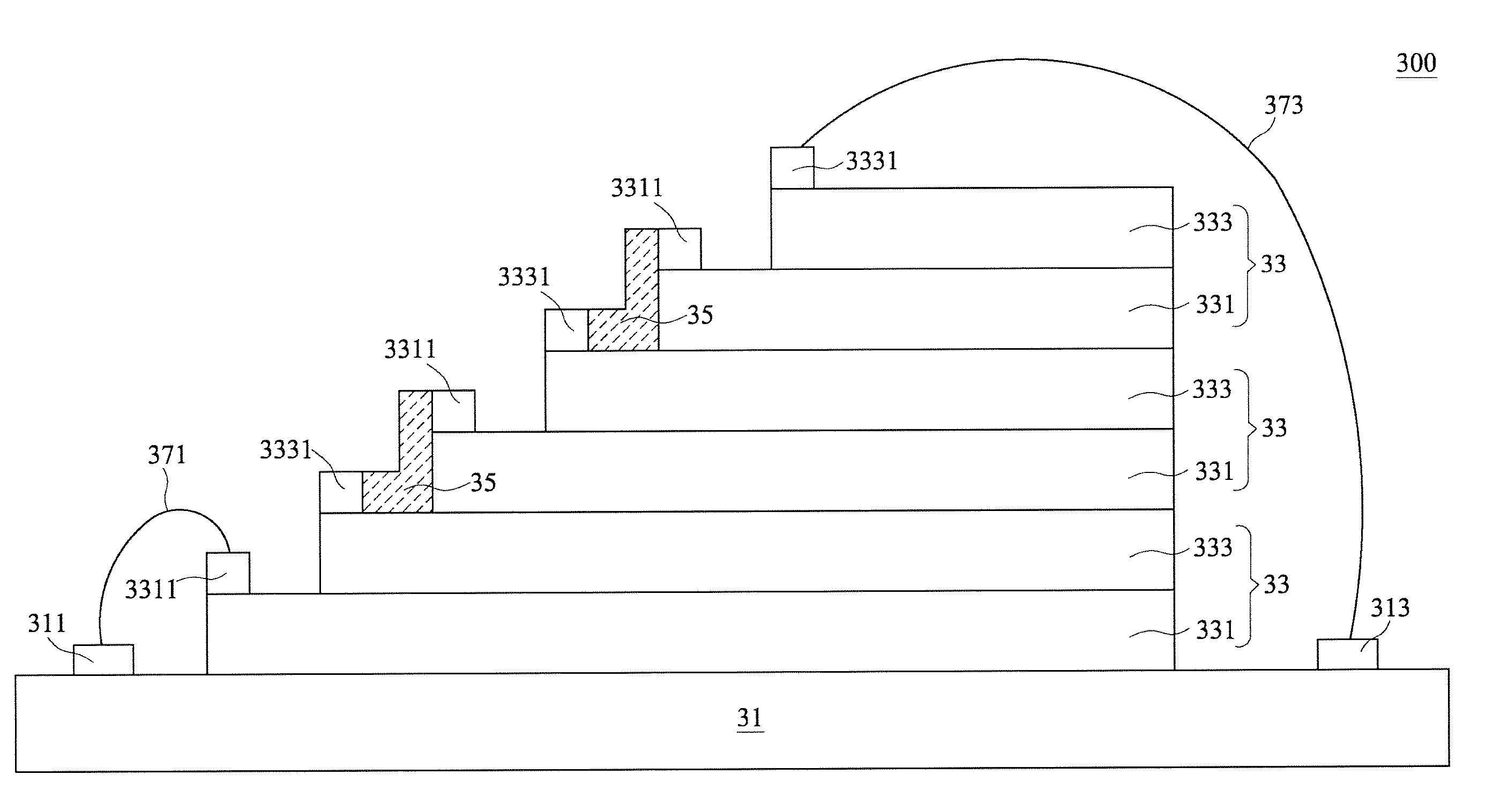
[0022]Referring to FIG. 3, there is shown a structural diagram of a stacked LED array structure according to one preferred embodiment of the present invention. As illustrated in the figure, an LED array 300 comprises a substrate 31 and a plurality of LED dies 33.

[0023]Each LED die 33, is stacked on the substrate 31 in turn, comprises a first semiconductor layer 331 and a second semiconductor layer 333, respectively. The first semiconductor layer 331 is an N-type semiconductor layer, while the second semiconductor. layer 333 is a P-type semiconductor layer.

[0024]When the deposition process is used, the second semiconductor layer 333 may be depositingly stacked on a part of surface of the first semiconductor layer 331 in each LED die 33, as well as the first semiconductor layer 331 of each LED die 33 may be depositingly stacked on a part of surface of the substrate 31 or a part of surface of the second semiconductor layer 333 of another LED die 33. Furthermore, the exposed surface at ...


PUM


Abstract

The present invention provides a stacked LED array structure, comprising a substrate and a plurality of LED dies stacked on the substrate in turn. Each LED die comprises a first semiconductor layer and a second semiconductor layer. The first semiconductor layer is provided thereon with a first electrode and stacked with the second semiconductor layer, while the second semiconductor layer is provided thereon with a second electrode and stacked with the first semiconductor layer of another LED die. The second electrode of each LED die is connected to the first electrode of another LED die in series via a metal layer to from an LED array. A plurality of LED dies may be stacked to be an LED array in a stacked manner, resulting in not only easy manufacturing, but also an effectively reduced volume for arranging the whole LED array.

Description

FIELD OF THE INVENTION[0001]The present invention is related to a light emitting diode array structure, particularly to a stacked light emitting diode array structure.BACKGROUND[0002]A light emitting diode (LED) is a semiconductor light emitting device, which is electroluminescent when forward bias is applied thereon. The recent LED has been developed to be operated with high-voltage alternating-current power supply (such as AC 110V / 220V, for example). Furthermore, the merits of low power consumption and long service life, compared with the electric lamp bulb (such as incandescent lamp, for example) or fluorescent tube (such as fluorescent lamp, for example), are provided for the LED. Therefore, the LED is used for illumination, instead of the electric lamp bulb or fluorescent tube, gradually.[0003]When the LED is applied to illumination, it is generally to connect a plurality of LEDs in series as an array, in such a way that the plurality of LEDs are used for luminescence, so as to...

Claims


Application Information

Patent Timeline
IPC IPC(8): H01L25/075
CPCH01L25/0756H01L25/0753H01L27/153H01L33/62H01L2224/48091H01L2224/48137H01L2224/45144H01L2924/00014H01L2924/00
Inventor TSAY, WEN CHINLAI, LI-HUNG
Owner MEILU SCI & TECH
Why Eureka
Try Eureka