Integrated inductor and integrated inductor fabricating method
- Summary
- Abstract
- Description
- Claims
- Application Information
AI Technical Summary
Benefits of technology
Problems solved by technology
Method used
Image

Examples
Embodiment Construction
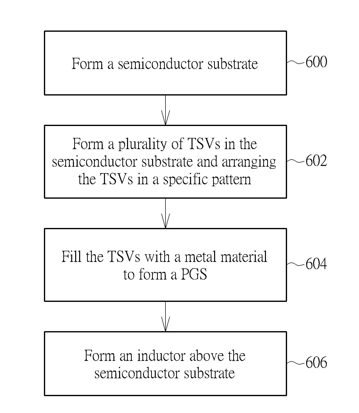
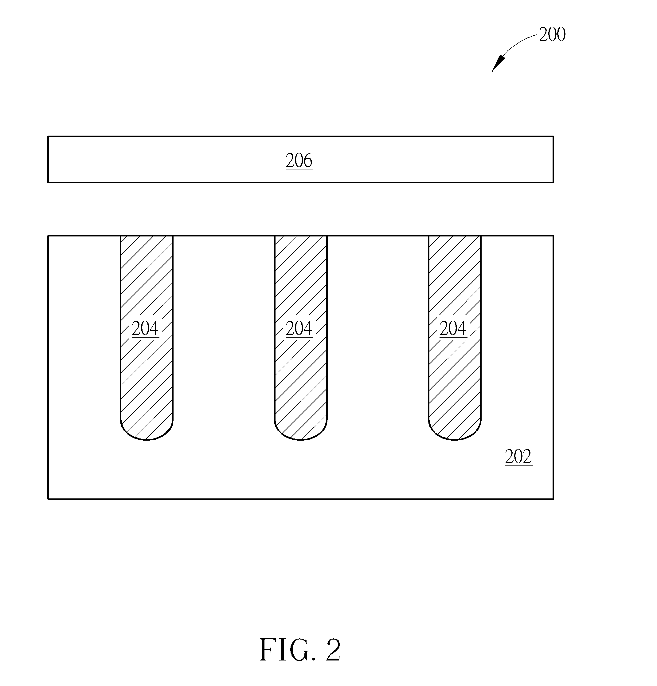
[0029]Please refer to FIG. 2. FIG. 2 shows a cross-sectional diagram of an integrated inductor 200 in accordance with a first embodiment of the present invention. As shown in FIG. 2, the integrated inductor 200 comprises: a semiconductor substrate 202, a plurality of deep trenches 204, and an inductor 206. The deep trenches 204 are formed in the semiconductor substrate 202 and arranged in a specific pattern (for example, as shown in FIG. 3, FIG. 3 shows a top-view structure diagram of the integrated inductor 200, but it is not meant to be a limitation of the present invention), and the deep trenches 204 are filled with a metal material (such as copper, aluminum, or gold) to form a patterned ground shield (PGS) 208, wherein width of the deep trenches 204 can be smaller than 20 micrometers, and depth of the deep trenches 204 can be smaller than 100 micrometers but greater than 20 micrometers. The inductor 206 can be formed above the semiconductor substrate 202. In addition, there can ...
PUM
 Abstract
Description
Claims
Application Information