This reconstruction process requires a great deal of
processing by a device, and is subject to failure if the
swipe movement and conditions are not optimum.
Such sensors however can be prohibitive in cost due to the large number of sensing points needed in the array.
These sensors, however, are based use 150 mm2 or more of
silicon area and are therefore cost prohibitive for many applications.
They are also delicate and fragile.
They are sensitive to
impact and even temperature changes, and thus are simply not durable enough for most applications, such as smart phones and other mobile electronic devices that are handled and sometimes dropped by users.
There are many applications for two dimensional image sensors as a particular example, and innovators have struggled with state of the art technology that has come short of desired features and functions.
Though accuracy and reliability are still important, cost of the
system components is very important.
The conventional placement sensors were and still are very expensive for one primary reason: they all used
silicon sensor surfaces (this is excluding optical sensors for this example, because they are simply too large and require more power than a portable device can afford to allocate, among other reasons, and thus they are generally not available in most commercially available devices).
These
silicon surfaces are very expensive, as the silicon material is as expensive as the material to make a computer
chip.
Thus, they were easy to spoof, or fake a
fingerprint with different deceptive techniques, and they also had poor performance when a user had dry fingers.
One key impediment to the development of low cost placement sensors has been the issue of
pixel density, and the
resultant requirement for a large number of interconnections between
layers of the sensor device.
While
semiconductor vias can be quite small, the cost for implementing a sensor in silicon has proven to be prohibitive, as mentioned above.
One further consideration is that at similar line densities, double-sided circuits with vias are several times more expensive per unit area than single sided, making high-density double sided circuits too expensive for low cost sensor applications.
For
laptop devices, adoption of the
swipe sensor was driven by cost.
Although this advance in the art enabled cheap durable
Swipe Sensors, it did not overcome the basic image reconstruction and ergonomics issues resulting from changing from a simple two dimensional placement format.
In most
swipe class sensors, the
fingerprint reconstruction process turned out to be a greater ergonomic challenge to users and more of a burden to
quality control engineers than initially expected.
Software training programs were written to help the user become more proficient, but different environmental factors and the inability of some to repeat the motion reliably gave
Swipe Sensors a reputation for being difficult to use.
Attempts to improve these reconstruction algorithms failed to produce equivalent statistical performance to placement sensors.
Development of sensors that take up less space on devices have been tried without much success.
These structures ended up consuming significant space in addition to the actual sensor area.
In the end, swipe sensors ended up taking up almost as much space as the placement sensors.
This was not a big problem for full size laptops, but is currently a substantial problem for smaller laptops and netbooks, mobile phones, PDAs, and other small devices like key fobs.
Real estate issues have become even more of an issue with
mobile device manufacturers who now require that the fingerprint sensor act also as a navigation device, like a mouse or touch-pad does in a
laptop.
The swipe sensor has proved to be a poor substitute for a mouse or touch pad due to the fact that they are constructed with an asymmetric array of pixels.
Swipe sensors do a good job of detecting motion in the normal axis of the finger swipe but have difficulty accurately tracking sideways motion.
Off axis angular movements are even more difficult to sense, and require significant processor resources to interpolate that movement with respect to the sensor line, and often have trouble resolving large angles.
It is clear that low cost two dimensional fingerprint sensor arrays would serve a market need, but present art has not been able to fill that need.
These prior art approaches cannot be configured into a low cost two dimensional array of sensing elements.
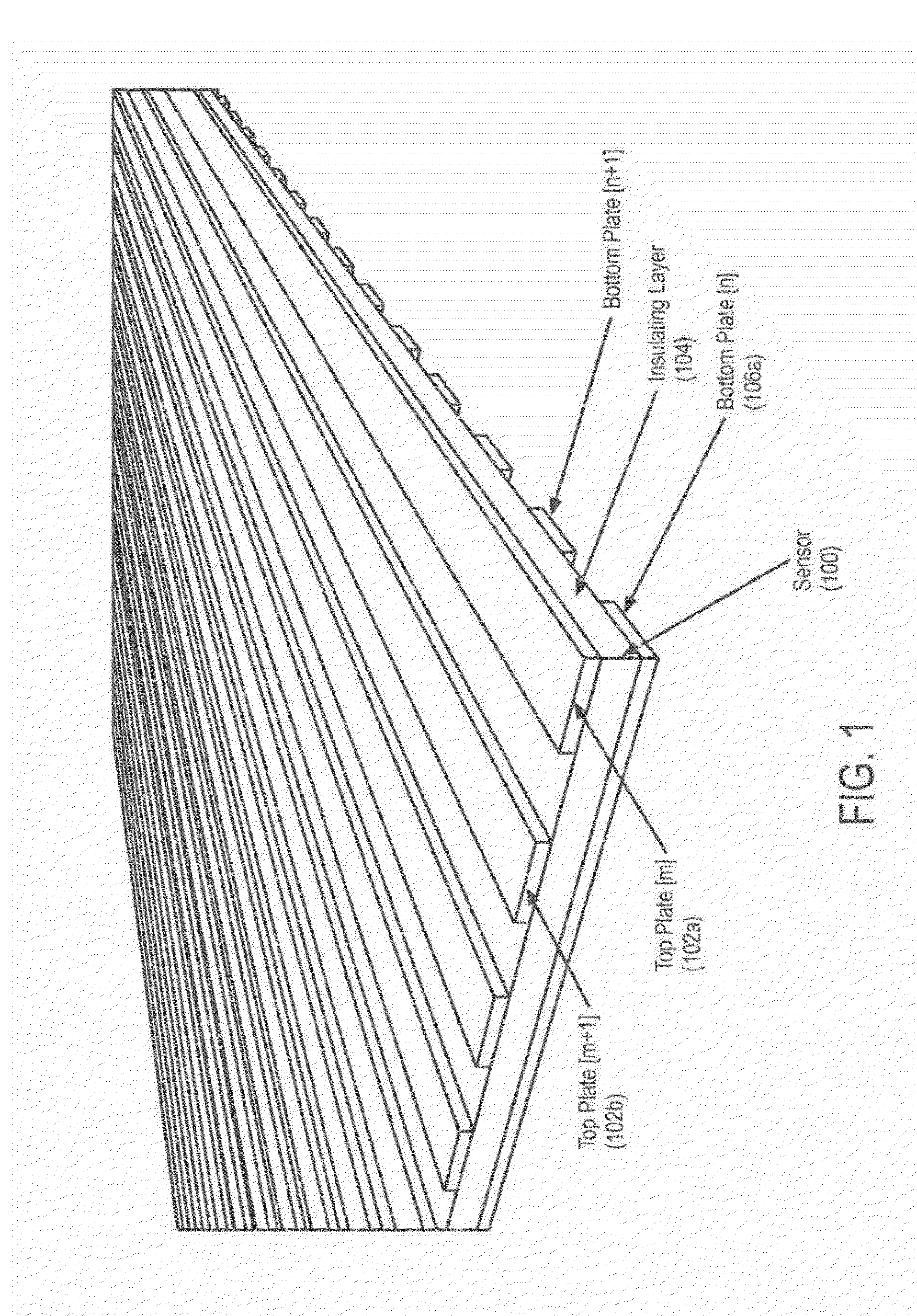
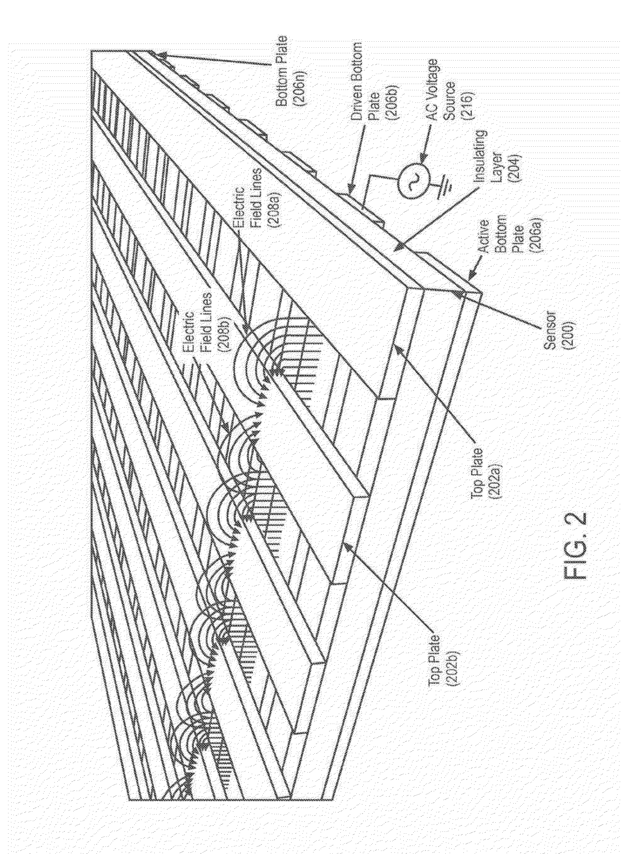
Many capacitive fingerprint sensors (for example U.S. Pat. Nos. 5,963,679 and 6,011,859) have plate structures that must be connected to the drive and sense
electronics with an interconnect density that is not practical for implementation other than using the
fine line multilayer routing capabilities of silicon chips and therefore require lots of expensive silicon die are as stated before.
Other sensors (for example U.S. Pat. No. 7,099,496) use off
chip sensing elements on a cheap
polymer film, but the sensor
cell architecture is inherently one dimensional and cannot be expanded into a two dimensional matrix.
Because
touchpad and touch screen devices consist of arrays of drive and sense traces and distinct sense electrodes, they are incapable of resolutions below a few hundred microns, making this technology unsuitable for detailed imaging applications.
These devices are capable of detecting finger contact or proximity, but they provide neither the spatial resolution nor the gray-scale resolution within the body of the object being sensed necessary to detect fine features such as ridges or valleys.
Thus, these devices operate at a
low resolution when sensing adjacent objects.

