Pulsed gas plasma doping method and apparatus

a plasma doping and plasma technology, applied in electrical devices, semiconductor devices, electric discharge tubes, etc., can solve the problems of difficult implementation of gas injection from showerheads opposite wafers/substrates, clustering of dopant species, and difficulty in providing conformal or uniform doping across substrates, etc., to prevent or reduce the possibility of ion induced damage to the substrate, the effect of low plasma potential

Active Publication Date: 2014-10-09
TOKYO ELECTRON LTD
View PDF7 Cites 11 Cited by
  • Summary
  • Abstract
  • Description
  • Claims
  • Application Information

AI Technical Summary

Benefits of technology

[0007]According to an example, when the flow is through the central injection port (or ports), the flow is not completely discontinued through the peripheral ports, and similarly, when the flow is through the peripheral ports, the flow is not completely discontinued to the central port. This avoids problems that can occur, for example, with backflow into the ports or deposits forming during the period in which they are not utilized as the primary location for injection. However, the flow through the ports during the time they are not being used as the primarily injection location is preferably kept small, preferably less than 20% of the total flow, more preferably less than 10% of the total flow or less than 5% of the total flow. Preferably, the flow through the non-primary port(s) is just sufficient so as to avoid backflow while also ensuring that the primary flow regime into the chamber is from the port through which the gas mixture is primarily being injected at a given time.
[0008]According to a preferred example, microwave energy is utilized to form and maintain the plasma with low plasma potential. The low plasma potential prevents or reduces the possibility of ion induced damage to the substrate. In addition, an RF power source can be applied to the substrate support or lower electrode upon which the substrate is placed during processing so as to provide an RF bias. This arrangement provides low energy ions for advantageous doping, particularly in combination with the alternating gas flow described above and in further detail hereinafter. The ion energy is sufficient, however, to amorphize or randomize the silicon surface of the substrate (with ions of the inert gas) and thereby allow the surface to receive and become saturated with the dopant.

Problems solved by technology

This central or peripheral gas injection is employed because using gas injection from showerheads opposite the wafer / substrate is difficult to implement in ECR, ICP, or microwave driven sources.
In doping a substrate, problems can arise in providing conformal or uniform doping across the substrate such as where the surface of the substrate is non-uniformly saturated with dopant across the substrate surface.
In certain areas excessive amounts of the dopant can be infused which can cause the dopant species to form clusters.
The consequence is loss of dopant in localized regions and the surface resistivity of the substrate will be non-uniform across the substrate.
In addition, if certain areas are insufficiently doped, the surface resistivity of the substrate will be non-uniform across the substrate.
Further, certain doping techniques can result in excessively high ion energies, which can undesirably damage features formed on the substrate that are being doped.
For example high energy ions can damage the corners of a Fin-FET (fin-like field effect transistors), or excessively penetrate into the substrate creating damaged material (silicon fin or gate structures).
Although cleaning steps can remove some damage, excessive damage can exceed amounts that will be removed in cleaning steps, e.g., as used as part of masking n and p (donor and acceptor) regions of die.
Doping of non-planar surfaces is also challenging in part because of poor view factors or geometries.

Method used


Image

  • Pulsed gas plasma doping method and apparatus
  • Pulsed gas plasma doping method and apparatus
  • Pulsed gas plasma doping method and apparatus

Examples


Embodiment Construction

[0016]With reference to the drawings, examples of embodiments of the invention will be described. It is to be understood that, although details and advantages of the invention are described with reference to illustrated examples, the invention can be practiced otherwise than as specifically described herein. For example, the invention could be practiced utilizing a subset or subsets of features described herein, and by utilizing certain advantages or benefits but not others. Accordingly, it is to be understood that the invention can be practiced otherwise than as specifically described herein.

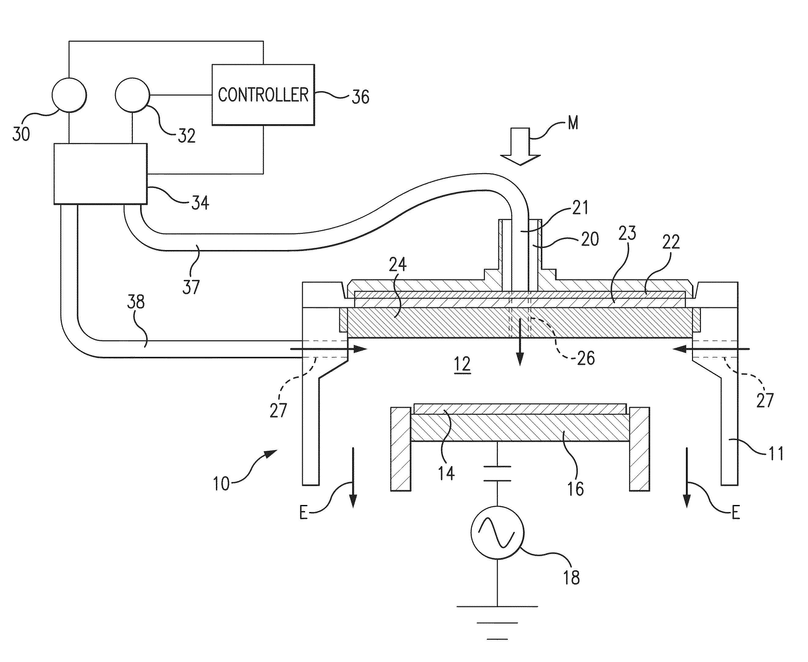
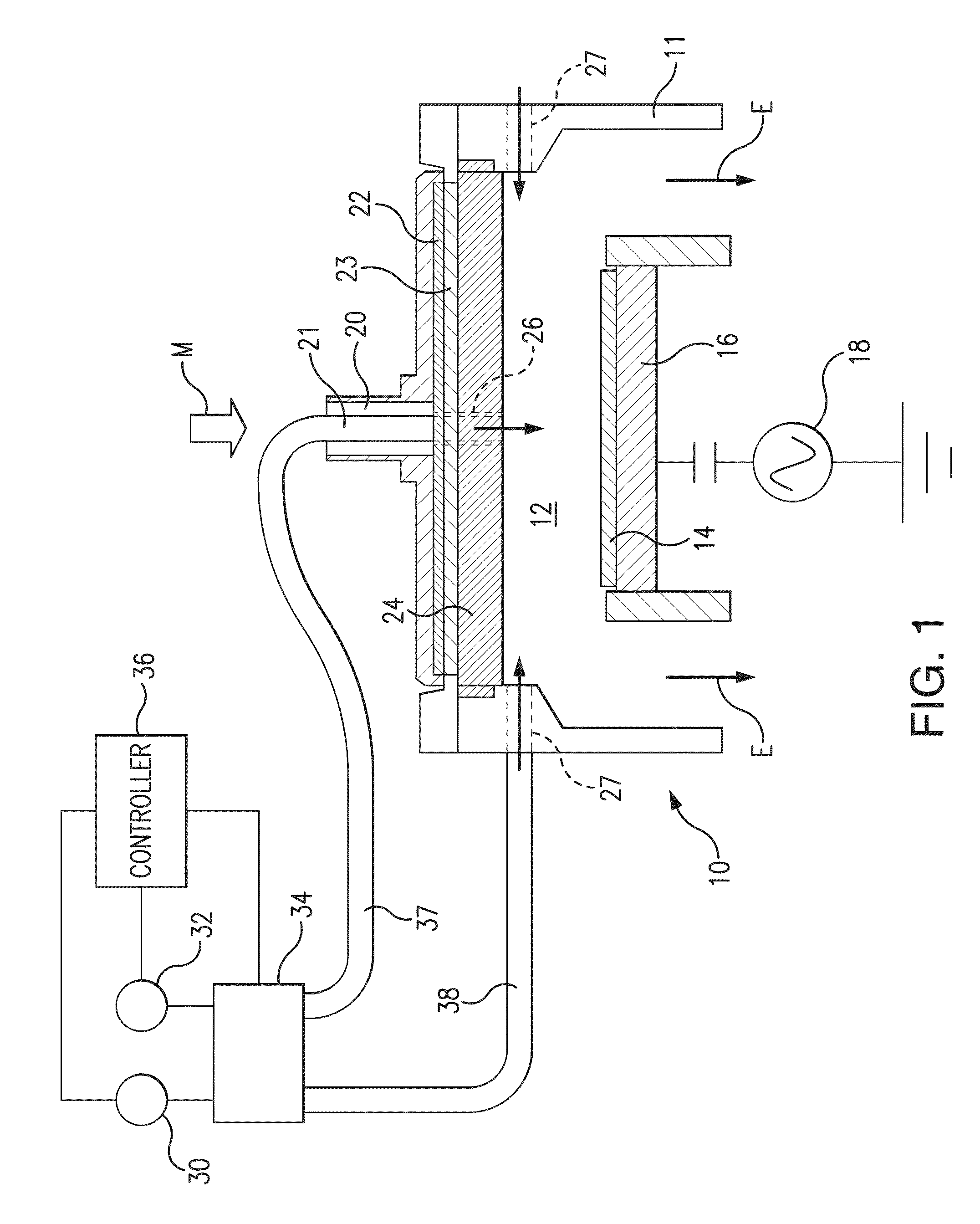
[0017]FIG. 1 illustrates a plasma processing apparatus which can be used in accordance with the present invention. As shown, the arrangement includes a processing chamber 10 enclosing a processing space 12 within which a plasma is generated. A wafer 14 is supported upon a substrate support 16. In a preferred arrangement, a bias, preferably an RF bias is applied by an RF source 18 to the wafer s...


PUM


Abstract

A method and apparatus for doping a surface of a substrate with a dopant, with the dopant being for example phosphine or arsine. The doping is performed with a plasma formed primarily of an inert gas such as helium or argon, with a low concentration of the dopant. To provide conformal doping, preferably to form a monolayer of the dopant, the gas flow introduction location is switched during the doping process, with the gas mixture primarily introduced through a center top port in the process chamber during a first period of time followed by introduction of the gas mixture primarily through peripheral or edge injection ports for a second period of time, with the switching continuing in an alternating fashion as the plasma process.

Description

CROSS REFERENCE TO RELATED APPLICATIONS[0001]This application claims priority to provisional application 61 / 808,321 filed Apr. 4, 2013, the entirely of which is incorporated herein by reference.TECHNICAL FIELD[0002]The invention relates to plasma doping, and particularly to a method and apparatus for doping the surface of a substrate. The invention is particularly advantageous in doping a silicon substrate having topographic structures such as fin shaped structures formed thereon.BACKGROUND OF THE INVENTION[0003]Doping refers to the insertion of atoms into a substrate to achieve a change in the substrate material properties. The properties can include, e.g., electrical mobility, index of refraction, surface reactivity, mechanical properties or more specifically electrical band structure. The most common application of doping is the implant of donor and acceptor species into electrical devices such as gate sources and drains. The process of doping can include an atom infusion step fo...

Claims


Application Information

Patent Timeline
Patent Type & Authority Applications(United States)
IPC IPC(8): H01L21/223H01J37/32
CPCH01L21/2236H01J37/32412H01J37/32449H01J37/3244H01L29/66803
Inventor VENTZEK, PETERNEMOTO, TAKENAOUEDA, HIROKAZUKOBAYASHI, YUUKIHORIGOME, MASAHIRO
Owner TOKYO ELECTRON LTD
Why Eureka
Try Eureka