Plasma processing apparatus

a processing apparatus and plasma technology, applied in the direction of plasma technique, coating, electric discharge lamps, etc., can solve the problems of difficult to generate intense inductively coupled plasma, weak excited magnetic field, difficult to prevent ion damage, etc., to achieve simple and accurate control of plasma processing uniformity, the effect of low plasma potential

Active Publication Date: 2013-10-08
TOKYO ELECTRON LTD +1
View PDF40 Cites 20 Cited by
  • Summary
  • Abstract
  • Description
  • Claims
  • Application Information

AI Technical Summary

Benefits of technology

[0012]In view of the above, the present invention provides a plasma processing apparatus capable of easily generating a stable high-density plasma having a low plasma potential and also capable of simply and accurately controlling uniformity of plasma processing of a substrate to be processed.

Problems solved by technology

Therefore, the voltage component remains in the spiral coil all the time, and a large amount of capacitively coupled components is generated in the plasma, which makes it difficult to prevent ion damage.
However, in case of using the spiral coil having the low inductance, the excited magnetic field becomes weak.
As a result, it is difficult to generate an intense inductively coupled plasma, and a plasma density decreases.
Thus, an inner line and an outer line divided by the point where the phase-voltage and the anti-phase voltage are switched have different reactances, and this makes it difficult to control the waveform to be symmetrical with respect to the point.

Method used


Image

  • Plasma processing apparatus
  • Plasma processing apparatus
  • Plasma processing apparatus

Examples


Embodiment Construction

[0040]The embodiments of the present invention will be described with reference to the accompanying drawings which form a part hereof. Further, like reference numerals will be given to like parts having substantially the same functions throughout the specification and the drawings, and redundant description thereof will be omitted.

[0041](Configuration Example of Plasma Processing Apparatus)

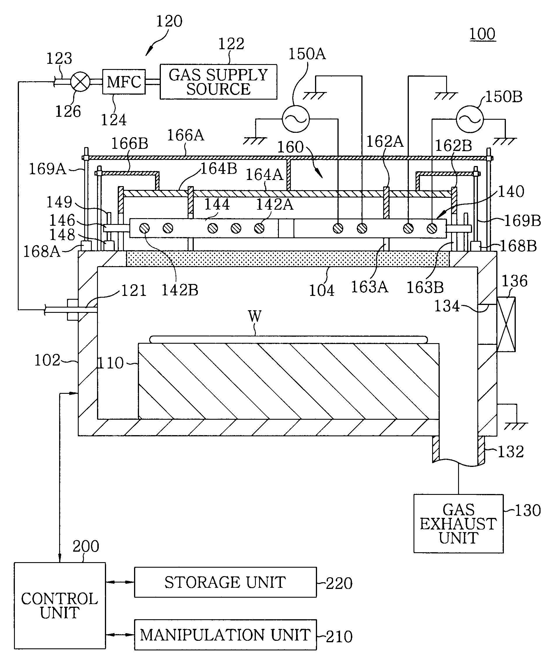
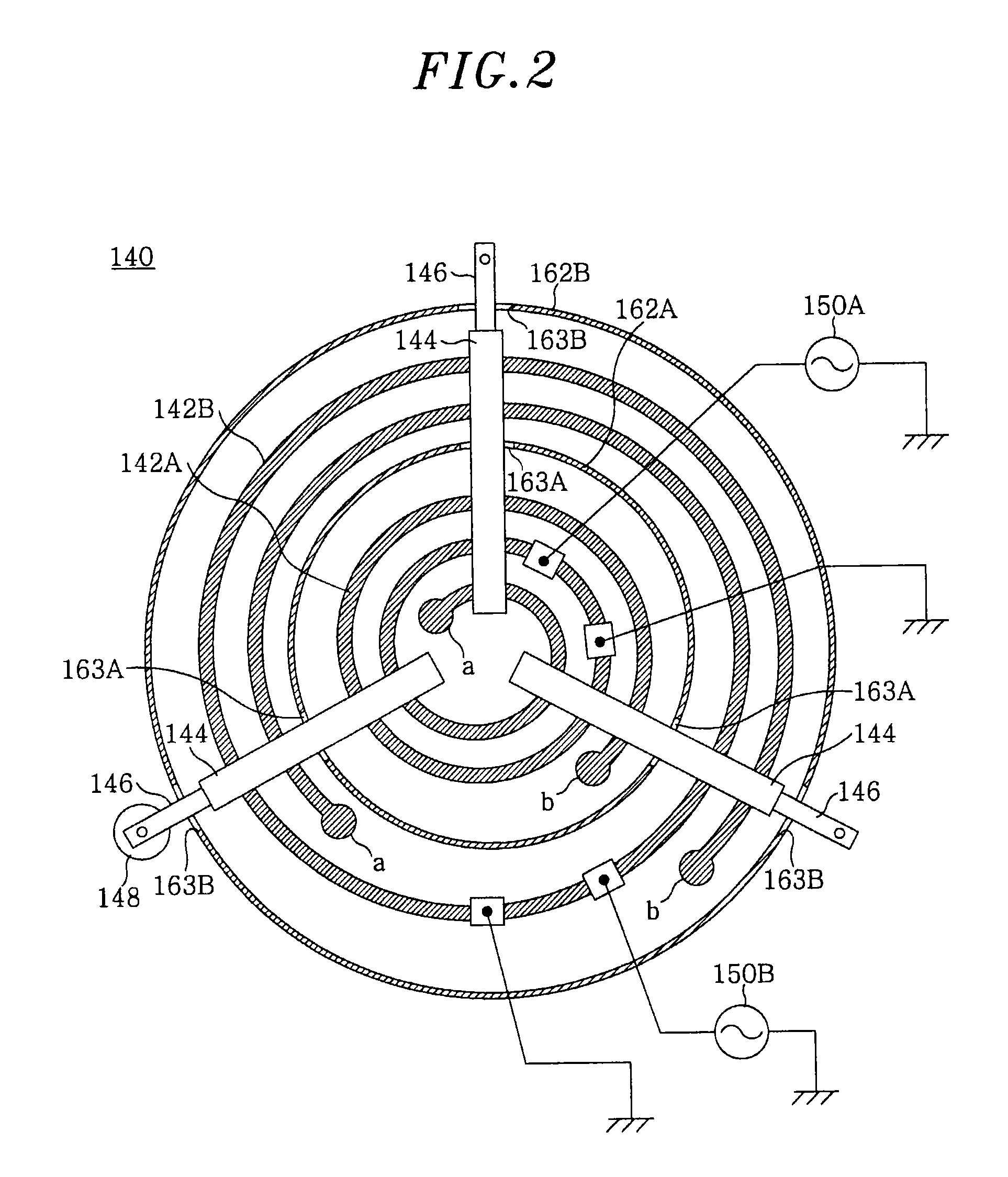
[0042]First, a configuration example of a plasma processing apparatus 100 in accordance with an embodiment of the present invention will be described with reference to the accompanying drawings. Herein, an inductively coupled plasma processing apparatus will be described as an example. The inductively coupled plasma processing apparatus performs a predetermined plasma processing on a substrate to be processed, e.g., a semiconductor wafer W by using a plasma of a processing gas which is excited in a processing chamber by applying a high frequency power to a planar high frequency antenna.

[0043]FIG. ...


PUM

PropertyMeasurementUnit
frequencyaaaaaaaaaa
frequencyaaaaaaaaaa
frequenciesaaaaaaaaaa

Abstract

A plasma processing apparatus, for performing a plasma processing on a target substrate by generating an inductively coupled plasma of a processing gas in a depressurized processing chamber, includes: a mounting table; a gas supply unit; a gas exhaust unit; a planar high frequency antenna disposed opposite to the mounting table with a plate-shaped dielectric member therebetween and a shield member covering the high frequency antenna. The high frequency antenna includes an inner antenna element provided at a central portion of a region above the plate-shaped dielectric member and an outer antenna element provided at an edge portion to surround a periphery of the inner antenna element. Further, two ends of each of the antenna elements are open ends and the antenna elements are grounded at central points thereof or points close thereto to resonate at ½ wavelengths of high frequencies from individual high frequency power supplies.

Description

CROSS-REFERENCE TO RELATED APPLICATIONS[0001]This application claims priority to Japanese Patent Application No. 2009-108752 filed on Apr. 28, 2009, the entire contents of which are incorporated herein by reference.FIELD OF THE INVENTION[0002]The present invention relates to a plasma processing apparatus for performing predetermined processing on a substrate to be processed by exciting a plasma of a processing gas.BACKGROUND OF THE INVENTION[0003]A plasma processing apparatus is used for various processing such as etching, ashing, plasma deposition and the like for a substrate to be processed, e.g., a semiconductor wafer, a flat panel display (FPD) substrate, or the like. As for the plasma processing apparatus, there is known, e.g., an apparatus in which a planar spiral coil having both ends grounded is provided above a dielectric member and a high frequency power supply is connected to a portion other than the both ends (see, e.g., Patent Document 1). Further, there is formed a sta...

Claims


Application Information

Patent Timeline
Patent Type & Authority Patents(United States)
IPC IPC(8): C23C16/00C23F1/00H01L21/306H05B31/26
CPCH01J37/321H01J37/3211H01J37/32174H05H1/46H01L21/31116H01L21/31122H01L21/32137H01L21/02H01L21/205H01L21/3065H01L21/76825H01L21/76826
Inventor NISHIMURA, EIICHIYONEYAMA, SHIMAO
Owner TOKYO ELECTRON LTD
Why Eureka
Try Eureka