Display device
- Summary
- Abstract
- Description
- Claims
- Application Information
AI Technical Summary
Benefits of technology
Problems solved by technology
Method used
Image

Examples
embodiments 1
(Overall Configuration)
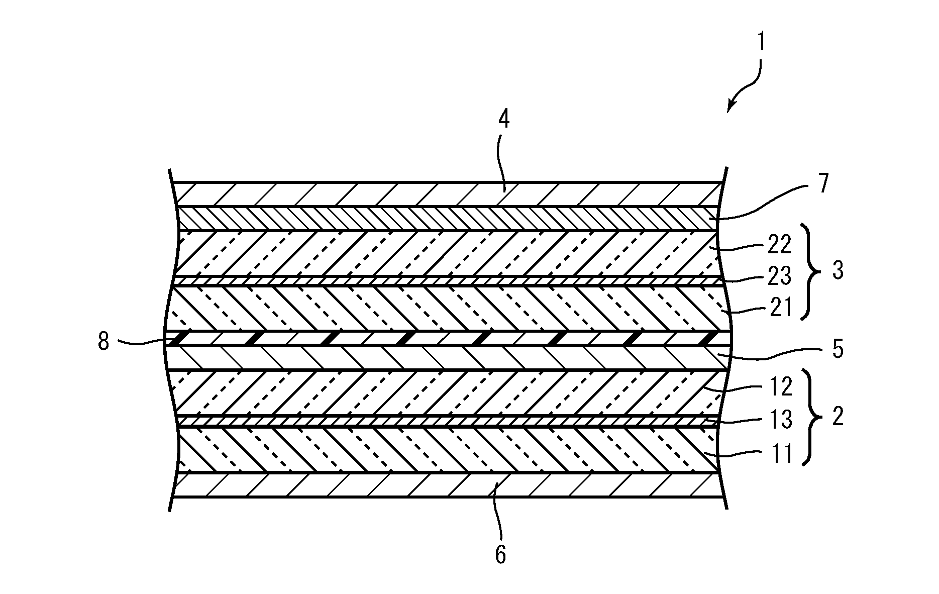
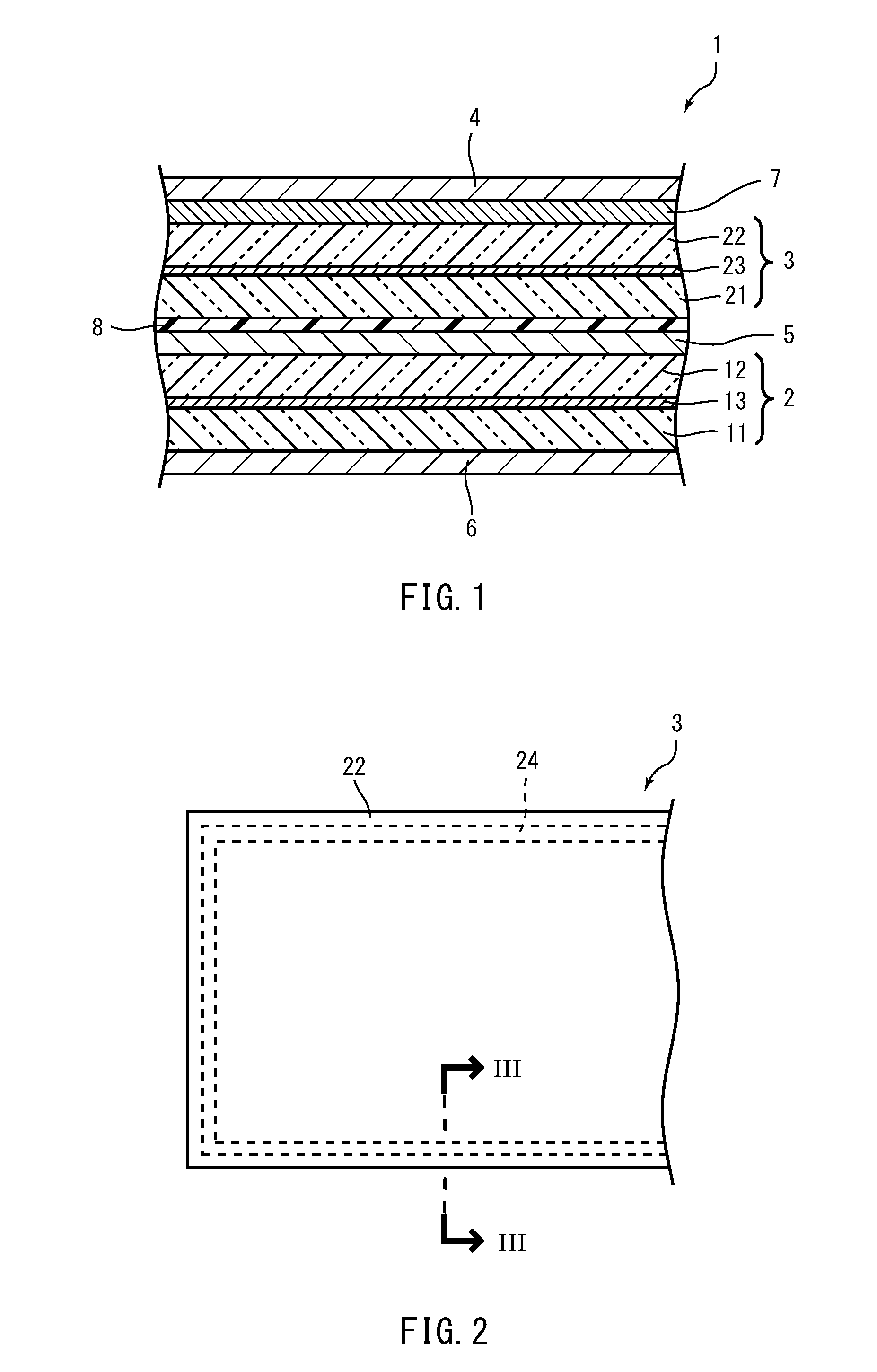
[0032]FIG. 1 illustrates a schematic configuration of a panel module 1 of a liquid crystal display device (display device) according to one embodiment of the present invention. This panel module 1 is composed of a plurality of members stacked in the thickness direction. More specifically, the panel module 1 includes a main panel 2 for displaying an image, a switching panel 3 for displaying a slit-like black-white image (stripe image), and three polarizing plates 4, 5, and 6 that are arranged with the main panel 2 and the switching panel 3 being interposed therebetween. The switching panel 3 is positioned on the viewing side of the main panel 2. It should be noted that, though not shown particularly, a backlight is provided on a back face of the panel module 1 (the side opposite to the viewing side).
[0033]As illustrated in FIG. 1, in the panel module 1, the polarizing plate 4, the retarder 7, the switching panel 3, the polarizing plate 5, the main panel 2, and...
embodiment 1
(Effects of Embodiment 1)
[0064]In the present embodiment, which has a configuration in which the switching panel 3 is arranged on the viewing side of the main panel 2, the polarizing plate 4 for converting incident light into linearly polarized light and the retarder 7 for converting the linearly polarized light into circularly polarized light are provided further on the viewing side with respect to the switching panel 3. With this configuration, even if light that is incident from the viewing side of the panel unit 1 is reflected by the switch panel 3, the reflected light can be blocked by the polarizing plate 4 and retarder 7. In other words, light incident from the viewing side of the panel unit 1 is converted by the polarizing plate 4 into linearly polarized light, and thereafter, it is converted by the retarder 7 into circularly polarized light. When the light is reflected by the switching panel 3, it is converted into circularly polarized light having an electric field vector ...
embodiment 2
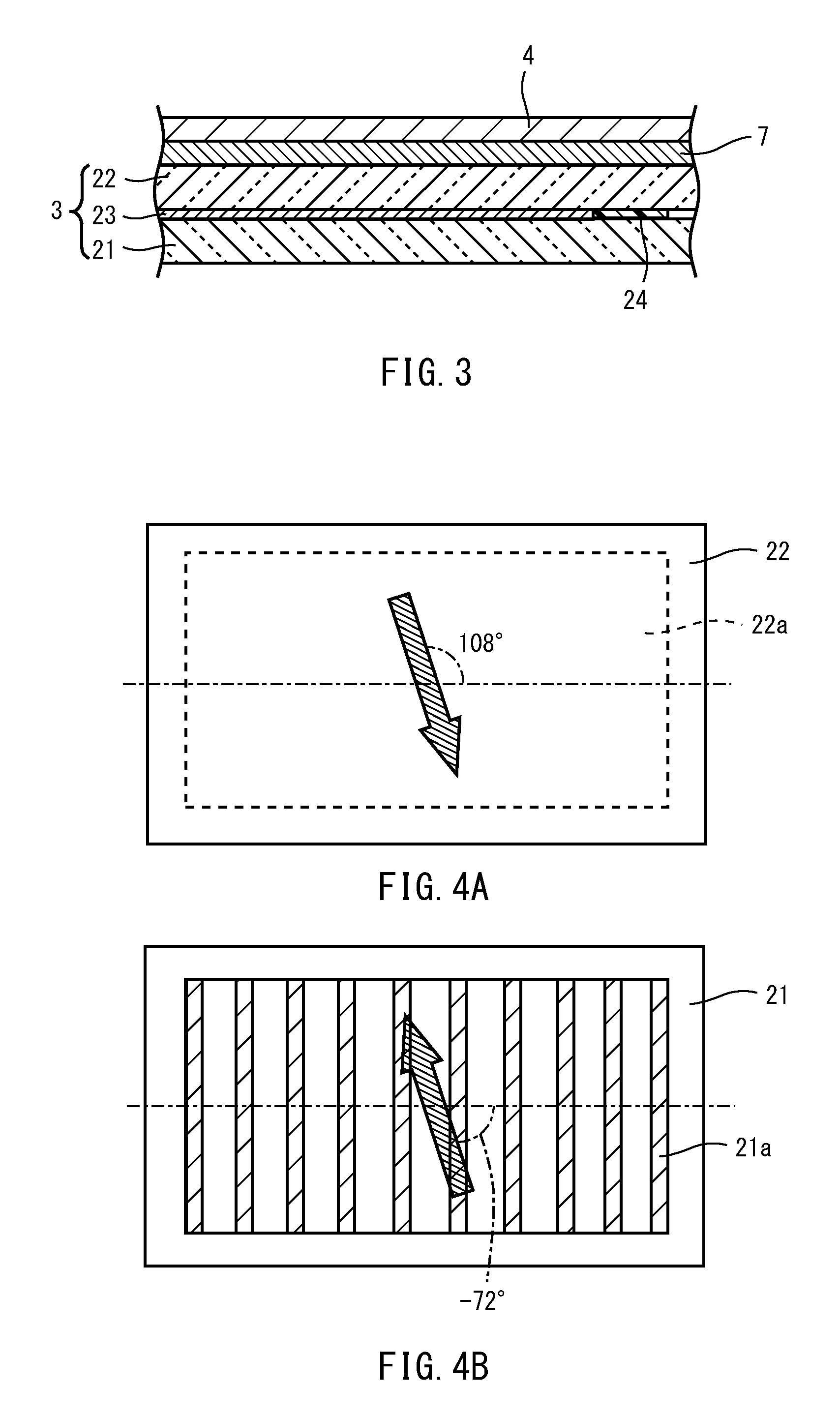
[0067]FIGS. 9A and 9B illustrate schematic configurations of a substrate 51 and a counter substrate 52 in a switching panel of a liquid crystal display device according to Embodiment 2 of the present invention. In Embodiment 2, the switching panel has a configuration different from the configuration in Embodiment 1 described above. Hereinafter, configurations identical to those in Embodiment 1 are denoted by the same reference numerals and descriptions thereof are omitted, and only those different from Embodiment 1 are described.
[0068]In the present embodiment, the panel unit is used in a state in which long sides of a switching panel illustrated in FIGS. 9A and 9B are directed to a longitudinal direction. Therefore, on the substrate 51 of the switching panel, there is formed a comb-shaped electrode 51a that has a plurality of slits extending in the lengthwise direction of the switching panel. It should be noted that on the counter substrate 52, as is the case with the counter subst...
PUM
 Abstract
Description
Claims
Application Information
PatSnap Eureka turns technology decisions into work you can execute. Powered by our Innovation Knowledge Graph, it runs expert workflows across engineering, life sciences, materials and intellectual property. Get your review-ready output in minutes.


