Resistive memory device and operation method thereof

a memory device and resistive technology, applied in the field of resistive memory devices, can solve the problems of pcram failure, limited lifespan of pcram, and degraded reliability of pcram

Active Publication Date: 2014-10-30
SK HYNIX INC
View PDF13 Cites 22 Cited by
  • Summary
  • Abstract
  • Description
  • Claims
  • Application Information

AI Technical Summary

Problems solved by technology

However, the GST material causes a phase-separation due to repeated crystallization and amorphization.
That is, it may be seen that a threshold voltage is lowered after the phase-separation of a phase-change material, for example, a GST material, and thus malfunction of the PCRAM may be caused.
As described above, the reliability of PCRAM is degraded and the lifespan of PCRAM is limited due to the phase-separation of the phase-change material, for example, a GST material, caused by the repeated operations.
However, when the refresh operation, including, for example, an erase operation, is performed in a separate operation period, a time for the refresh operation may be additionally needed, and thus write latency may be increased.

Method used


Image

  • Resistive memory device and operation method thereof
  • Resistive memory device and operation method thereof
  • Resistive memory device and operation method thereof

Examples


Embodiment Construction

”.

BRIEF DESCRIPTION OF THE DRAWINGS

[0032]The above and other aspects, features and other advantages of the subject matter of the present disclosure will be more clearly understood from the following detailed description taken in conjunction with the accompanying drawings, in which:

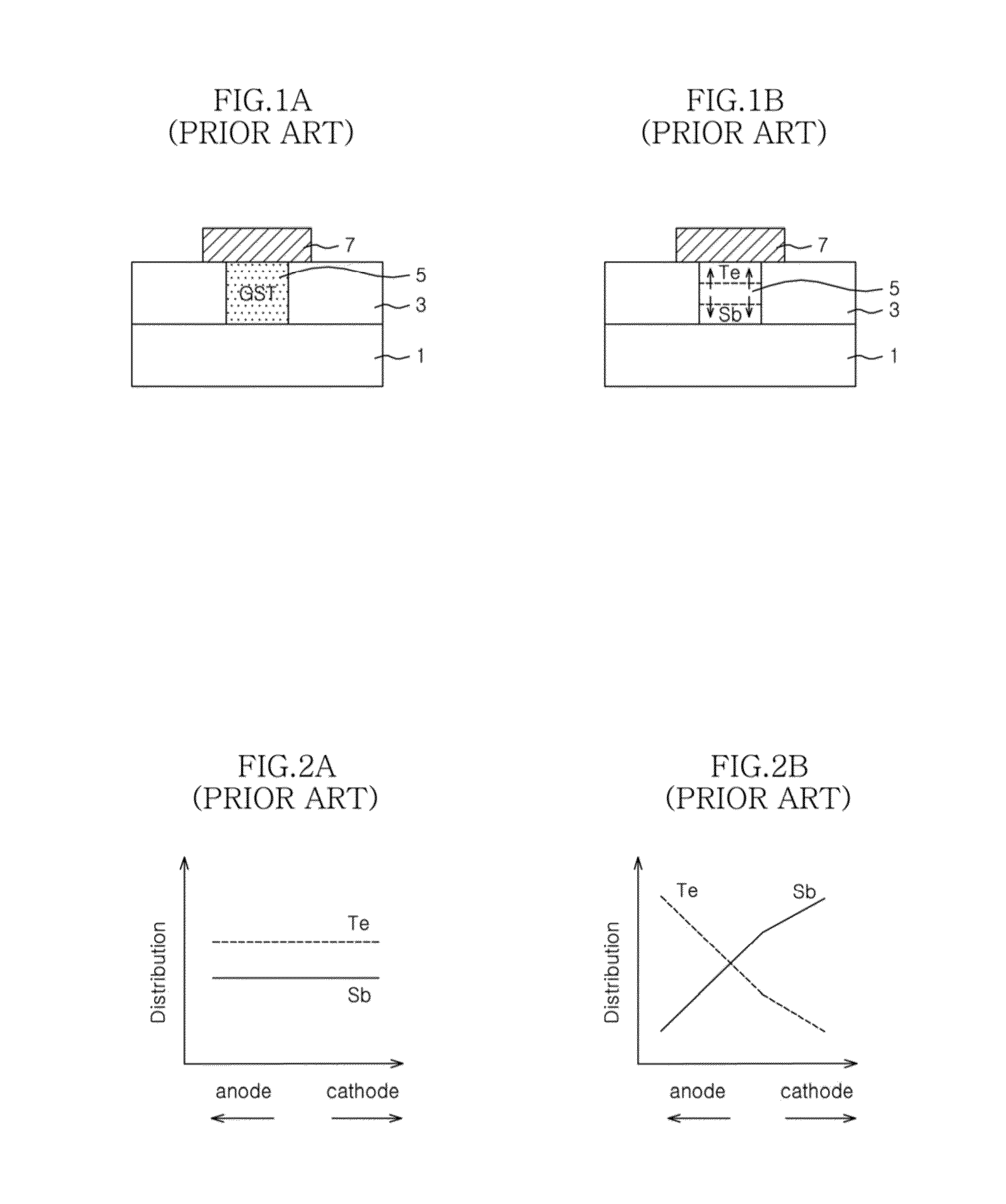
[0033]FIGS. 1A and 1B are cross-sectional views for explaining characteristics of a conventional PCRAM;

[0034]FIGS. 2A and 2B are distribution diagrams for explaining phase-separation of a GST material;

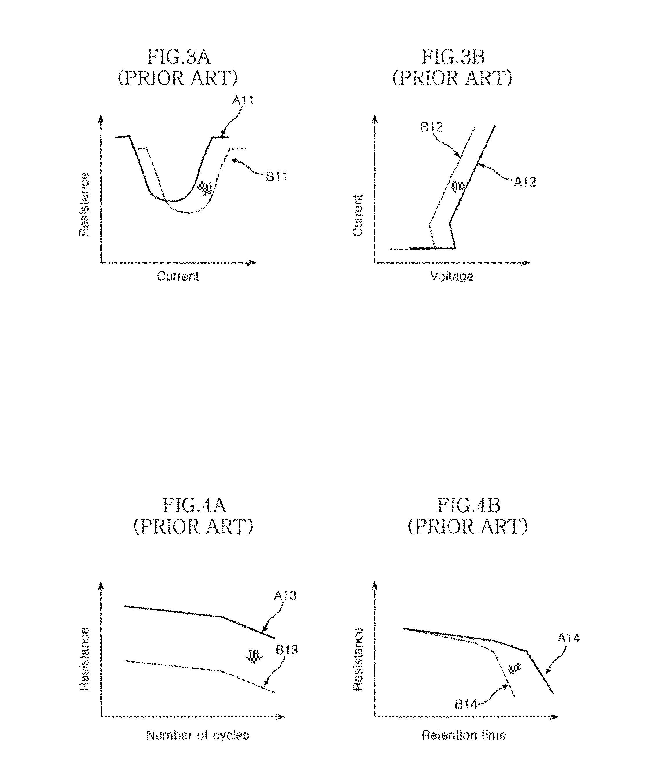
[0035]FIGS. 3A and 3B are characteristic diagrams illustrating current and voltage characteristics changes of a PCRAM due to repeated write operations;

[0036]FIGS. 4A and 4B are characteristic diagrams illustrating reliability change of a PCRAM due to repeated write operations;

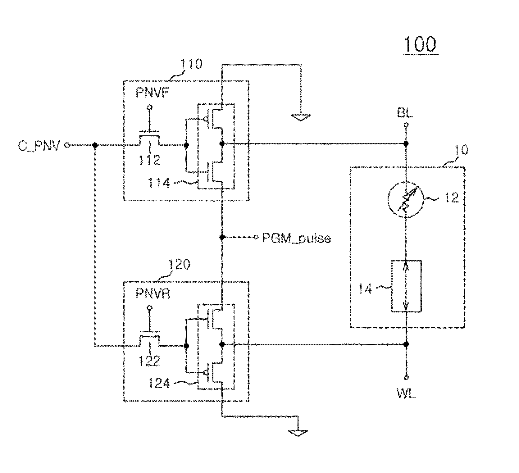
[0037]FIG. 5 is a diagram illustrating a unit memory cell of a resistive memory device according to an exemplary embodiment of the inventive concept;

[0038]FIG. 6 is a block diagram illustrating a path setting circuit of a resistive memor...


PUM


Abstract

A resistive memory device includes a memory cell array including a unit memory cell coupled between a word line and a bit line, wherein the unit memory cell includes a data storage material and a non-silicon-substrate-based type bidirectional access device coupled in series, a path setting circuit coupled between the bit line and the word line, suitable for providing a program pulse toward the bit line or the word line based on a path control signal, a forward write command, and a reverse write command, and a control unit suitable for providing a write path control signal, a forward program command, and a reverse program command based on an external command signal.

Description

CROSS-REFERENCES TO RELATED APPLICATION[0001]The present application claims priority under 35 U.S.C. §119(a) to Korean application number 10-2013-0046089, filed on Apr. 25, 2013, in the Korean Intellectual Property Office, which is incorporated herein by reference in its entirety.BACKGROUND[0002]1. Technical Field[0003]The inventive concept relates to a semiconductor integrated circuit, and more particularly, to a resistive memory device.[0004]2. Related Art[0005]Resistive memory devices use a resistive material of which a resistance is sharply changed based on an applied voltage to switch at least two different resistance states. There are typically a phase-change random access memory (PCRAM), a resistive random access memory (ReRAM), and a magnetoresistive random access memory (MRAM) as the resistive memory devices.[0006]Among the resistive memory devices, the PCRAM determines data to be stored in the selected memory cell based on a crystalline state of a phase-change material. By...

Claims


Application Information

Patent Timeline
Patent Type & Authority Applications(United States)
IPC IPC(8): G11C13/00
CPCG11C13/003G11C13/0004G11C13/0007G11C13/0064G11C2213/73G11C2013/0073G11C2013/0092G11C2213/15G11C13/0069G11C13/00G11C16/10G11C11/5678G11C13/0033G11C13/004G11C13/0097
Inventor PARK, HAE CHANKIM, MYOUNG SUBLEE, SE HOLEE, SEUNG YUN
Owner SK HYNIX INC
Why Eureka
Try Eureka