[0043]In the description which follows, like parts are marked throughout the specification and drawings with the same reference numerals. The drawings are not necessarily to scale and the proportions of certain parts have been exaggerated to better illustrate details and features of embodiments of the invention.
DETAILED DESCRIPTION
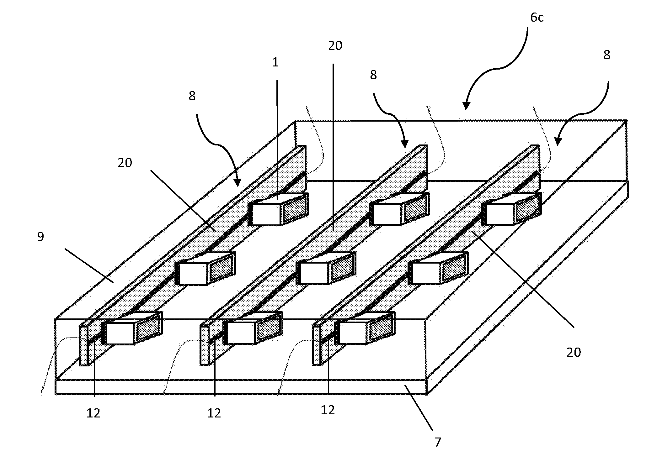
[0044]Referring to FIGS. 3 and 4, a side view and a schematic representation, respectively, of a lighting panel 6 in accordance with an embodiment of the present invention is presented. The lighting panel 6 can be seen to comprise a substrate 7 made from a transparent polymer sheet, such as polyester or polycarbonate and having a refractive index ns between 1.50 and 1.61.
[0045]Located on top of the substrate 7 are three, 3×1 arrays of light sources 8, further details of which are provided below.
[0046]Covering the 3×1 arrays of light sources 8, and the remaining area of the top surface of transparent substrate 7, is a guide layer 9, also formed from a transparent plastic polymer e.g. silicone, and having a refractive index ng between 1.41 and 1.56. The refractive indices of the transparent substrate and the transparent guide layer 9 are selected such that they satisfy the inequality ns≧ng. As a result, and as shown in FIG. 3, light 10 generated by the 3×1 arrays of light sources is initially coupled into the transparent guide layer 9 so as to propagate in a direction substantially parallel to a plane defined by the transparent substrate 7. Since the refractive index of the transparent substrate 7 is selected to be equal or higher than that of the transparent guide layer 9, the generated light 10 is guided within the combined structure formed by the transparent substrate 7 and the transparent guide layer 9 due to the effects of total internal reflection. Therefore, the transparent substrate 7 and the transparent guide layer 9 form a composite structure that acts as the guiding media for the light 10 generated by the encapsulated LED light sources 1.
[0047]Located on the lower surface of the transparent substrate 7 are a plurality of scattering structures 11. For ease of understanding a single pyramid style scattering structure 11 is presented. The scattering structures 11 may comprise alternative shaped structures or compositions e.g. a patterned layer of a reflecting ink. When the light 10 has propagated as far as the scattering structure 11 it interacts with this structure so disrupt or overcome the effects of total internal reflection. As a result the light 10 is redirected and so exits the device via the top surface of the transparent guide layer 9, so providing a backlighting function. It will be readily apparent to those skilled in the art that the scattering structures 11 may alternatively be located on the top surface of the transparent guide layer 9. In this embodiment the redirected light 10 will exit the device via the lower surface of the transparent substrate 7.
[0048]Each of the 3×1 arrays of light sources 8 can be seen to comprise three top emitting LEDs 1 mounted on an electrical tracking 12. Significant however, is the fact that all of the top emitting LEDs are side mounted on the electrical tracking 12 i.e. the generated “warm white” propagating from the light emitting areas 4 is now emitted in a direction substantially parallel to the plane of the transparent substrate 7. In the presently described embodiment globules of electrical conducting material 13 provides the means for electrically and mechanically connecting the side mounted top emitting LEDs to the respective electrical tracking 12. The electrically conducting material 13 comprises a silver loaded epoxy however it may alternatively comprise any other electrically conducting material that can be dispensed or printed in the desired volumes before being fixed in place e.g. by a curing process.
[0049]The above described lighting panel 6 provides a novel means for providing “warm white” illumination, backlighting, signage or displays. The apparatus employs standard top emitting LEDs 1 but does not require the employment of one or more reflecting structures so as to redirect light emitted from top emitting LEDs so as to propagate in a direction substantially parallel to the plane of the transparent substrate 7 on which they are mounted. As a result the described lighting panels 6 exhibit significantly higher optical efficiencies when compared with those devices known in the art. In addition they also offer a solution that can be manufactured on a commercial scale while offering acceptable levels of reliability.
[0050]A method of producing a lighting apparatus 6a in accordance with an alternative embodiment of the present invention will now be described with reference to FIG. 5 and FIG. 6. The first step 14 involves the deployment of an electrical tracking 12 on the top surface of the transparent substrate 7. Two contact pads (not explicitly shown) are then attached to the electrical tracking 3 at the desired location for the LED 1.
[0051]The second step 15 involves depositing some adhesive 16 on the top surface of the transparent substrate 7 at the desired position for locating the LED 1.
[0052]The third step 17 involves placing the top emitting LED 1 on top of the adhesive such that it is side mounted on the electrical tracking 12 i.e. the generated “warm white” propagating from the light emitting area 4 is arranged such that it will be emitted in a direction substantially parallel to the plane of the transparent substrate 7. A pick and place, surface-mount machine may be employed to complete this stage of the process.
[0053]The fourth step 18 comprises the application of two globules of conducting material 13 onto the electrical pads in the vicinity of the electrical contacts 3 for the LED 1. Each globule 13 then connects the respective electrical pad to the LED 1. The globules of conducting material 13 are then cured or reflowed to form a solid mechanical and electrical connection between the electrical pads on the tracking 12 of the transparent substrate 7 and the contacts 3 of the LED 1, thus allowing electrical power to be delivered to the LED 1.
[0054]The final step 19 comprises the application of the transparent guide layer 9 on top of the transparent substrate 7, so as to encapsulating the LED 1. This may be achieved by applying the desired liquid polymer to the top surface of the substrate 7 by printing, stenciling or dispensing the liquid polymer. By correctly selecting the refractive indices for the transparent substrate 7 and the guide layer 9 these components form a composite structure that acts as the guiding media for the light 10 generated by the encapsulated LED 1.
[0055]Referring to FIGS. 7 and 8, a side view and a schematic representation, respectively, of a lighting panel 6b and 6c in accordance with alternative embodiments of the present invention are presented. The lighting panels 6b and 6c can again be seen to comprise a substrate 7 made from a transparent polymer sheet, such as polyester or polycarbonate and having a refractive index ns between 1.50 and 1.61.
[0056]Located on top of the substrate 7 are three, 3×1 arrays of light sources 8b, further details of which are provided below.
[0057]Covering the 3×1 arrays of light sources 8, and the remaining area of the top surface of transparent substrate 7 is a guide layer 9, again formed from a transparent plastic polymer, and having a refractive index ng between 1.46 and 1.56. The refractive indices of the transparent substrate 7 and the transparent guide layer 9 are again selected such that they satisfy the inequality ns≧ng such that the transparent substrate 7 and the transparent guide layer 9 form a composite structure that acts as the guiding media for the light 10 generated by the encapsulated LED light sources 1.
[0058]Located on the lower surface of the transparent substrate 7 are a plurality of scattering structures 11.
[0059]In these embodiments, each of the 3×1 arrays of light sources 8b can again be seen to comprise three top emitting LEDs 1. However, in the presently described embodiments the LEDs 1 are initially mounted in a conventional manner onto a printed circuit board (PCB) 20. This is achieved via two contact pads (not explicitly shown) that are attached to the electrical tracking at the desired location for positioning of the LED 1. Solder reflow or conducting epoxy may be employed to mechanically and electrically connect the contacts 3 of the LED 1 to the contact pads. The PCB 20 may comprise a transparent material e.g. polyethylene terephthalate (PET) or polyimide or an opaque material e.g. FR-4 (woven glass and epoxy) or aluminium.
[0060]As can be seen from FIGS. 7 and 8 the PCBs 20 are side mounted into the top surface of the transparent substrate 7 before the guide layer 9 is cured and hardened so as to encapsulate the LEDs 1. In this way the top emitting LEDs 1 are again mounted on the substrate 7 in a side emitter configuration within the composite light-guiding structure with electrical connections to the LEDs 1 being made through the electrical tracking 12 on the substrate 7.
[0061]In FIG. 7 the PCB 20 can be seen to protrude from the top surface of the guide layer 9 while in the embodiment of FIG. 8 the PCBs 20 are fully encapsulated. In both embodiments the PCBs 20 are found to provide a means for enhanced dissipation of the heat generated by the LEDs 1, although this effect is more significant within the projected PCB 20 configuration of FIG. 7. Being able to increase the dissipation of the heat generated by the LEDs 1 has obvious benefits for the reliability of the lighting panels 6c and 6d.
[0062]FIG. 9 presents a schematic representation of a method of production of a lighting panel 6d in accordance with an alternative embodiment of the present invention while FIG. 10 presents a top view of the lighting panel 6d produced by this method. This embodiment is similar to that described above with reference to FIGS. 7 and 8 however, instead of mounting the LED 1 on a conventional PCB 20 the LED 1 is instead mounted on a daughterboard 21. The transparent substrate 7 is also adapted such that the daughterboard 21 can be mechanically connected to the substrate 7 via plugs, sockets, pins or other similar mechanical connecting means.
[0063]The manufacture of the daughterboard 21 can be by a simple and low cost printed circuit board manufacturing method. Importantly, the daughterboard 21 is manufactured so as to have electrical pads (not explicitly shown) on the two separate surfaces, one set adapted for electrical connection to the LED 1 and the other adapted for connection to the electrical tracking 12 on the top surface of the transparent substrate 7. Solder reflow or conducting epoxy may be employed to achieve the desired electrical connections between these components.
[0064]As will be readily apparent to the skilled reader the presently described embodiment provides an alternative means for mounting the top emitting LEDs 1 on the substrate 7 in a side emitter configuration within the composite light-guiding structure with electrical connections to the LEDs 1 again being made through the electrical tracking 12 on the substrate 7.
[0065]As with the above described embodiments that employ PCBs 20 the presence of the daughterboards 21 within the presently described embodiments also provide a means for enhanced dissipation of the heat generated by the LEDs 1.
[0066]In a yet further alternative embodiment shown in FIG. 11, and generally depicted by reference numeral 6e, the relative refractive indices between the transparent substrate 7 and the guide layer 9 may be selected such that they satisfy the inequality ns g. The light 10 generated by the 3×1 arrays of light sources 8 is again initially coupled into the transparent guide layer 9 so as to propagate in a direction substantially parallel to a plane defined by the transparent substrate 7. However since the refractive index of the transparent substrate 7 is selected to be less than that of the transparent guide layer 9, the generated light 10 is guided wholly within the transparent guide layer 9 due to the effects of total internal reflection. In the presently described embodiment it will be recognised by the skilled reader that the plurality of scattering structures 11 (omitted from this Figure for ease of understanding) are required to be located on the top surface of the guide layer 9. As a result the light 10 is redirected as described previously and so exits the device 6e via the lower surface of the substrate 7, so as to provide the desired backlighting function.
[0067]Although described in relation to top emitting LEDs that emit white light it will be apparent to the skilled reader that the above described embodiments may employ different coloured LEDs. This may involve employing only LEDs that emit a single colour within the lighting panel or alternatively LEDs that emit different colours so that a combination of lighting effects can be produced.
[0068]The above described embodiments provide a lighting panel suitable for providing “warm white” backlighting for a range of products e.g. mobile phone LCD displays. The lighting panels are able to employ standard top emitting LEDs and so avoid the need for significant redesign of the side emitting LEDs known in the art. Furthermore, the described embodiments do not require the employment of one or more reflective components and so exhibit significantly greater optical efficiencies when compared to those systems known in the art.
[0069]A further advantage of some of the above described embodiments is the fact that the PCD and daughterboards employed within the apparatus offer enhanced dissipation of the heat generated by the LEDs. Being able to increase the dissipation of the heat generated by the LEDs has obvious benefits for the reliability of the described lighting panels.
[0070]As a result of these combined advantages the described lighting panels offer a means for “warm white” backlighting of products that can be manufactured on a commercial scale while offering acceptable levels of reliability.
[0071]A lighting panel and method of production thereof is described. The lighting panel comprises a transparent substrate, upon a first surface of which are mounted one or more light sources is described. The lighting panel further comprises a guide layer wherein the guide layer is arranged so as to encapsulate the one or more light sources upon the first surface. The one or more light sources comprise top emitting LEDs side mounted upon the first surface. In this way the described apparatus provides an optically efficient means for providing “warm white” backlighting of products that can be manufactured on a commercial scale while offering acceptable levels of reliability.
[0072]The foregoing description of the invention has been presented for purposes of illustration and description and is not intended to be exhaustive or to limit the invention to the precise form disclosed. The described embodiments were chosen and described in order to best explain the principles of the invention and its practical application to thereby enable others skilled in the art to best utilise the invention in various embodiments and with various modifications as are suited to the particular use contemplated. Therefore, further modifications or improvements may be incorporated without departing from the scope of the invention as defined by the appended claims.