Single layer 3D tracking semiconductor detector

a semiconductor detector and single-layer technology, applied in the field of pixel detectors, can solve the problems of providing two-dimensional information of radiation fields, and achieve the effects of simple and affordable means, moderate power consumption of pixel detectors, and robustness

Active Publication Date: 2014-11-13
CZECH TECH UNIV IN PRAGUE
View PDF2 Cites 18 Cited by
  • Summary
  • Abstract
  • Description
  • Claims
  • Application Information

AI Technical Summary

Benefits of technology

[0029]In a preferred embodiment, the evaluation unit is configured to account for the time-over-threshold information associated with each read-out circuit such as to correct for a time-walk in the time difference information. In the art, the “time-walk” refers to an effect that occurs if simple threshold triggering is applied to signals having rise times that are considerably longer than the desired time resolution, and where signals of different amplitude are considered. For example, an incoming signal with comparatively large amplitude will reach the threshold earlier than an incoming signal having smaller amplitude but an identical rise time even if the maxima of the two signals were simultaneous. This timing difference that is essentially due to the different amplitudes of the signal is called “time-walk”. However, the time-walk can be corrected for if the amplitude of the signal is known, which in turn can be discerned from the time-over-threshold information. Alternatively, it is also possible to use a constant fraction discriminator. In this case, no time-walk will occur, as the timing of the signal independent of the pulse height.
[0030]As is apparent from the above discussion, the new pixel detector allows for obtaining 3-dimensional information employing only

Problems solved by technology

While such pixel detectors offer remarkable advantages with regard to robustness, sensitivity and v

Method used


Image

  • Single layer 3D tracking semiconductor detector
  • Single layer 3D tracking semiconductor detector
  • Single layer 3D tracking semiconductor detector

Examples


Embodiment Construction

[0037]For the purposes of promoting an understanding of the principles of the invention, reference will now be made to the preferred embodiment illustrated in the drawings and specific language will be used to describe the same. It will nevertheless be understood that no limitation of the scope of the invention is thereby intended, such alterations and further modifications in the illustrated device and method and such further applications of the principles of the invention as illustrated therein being contemplated therein as would normally occur now or in the future to one skilled in the art to which the invention relates.

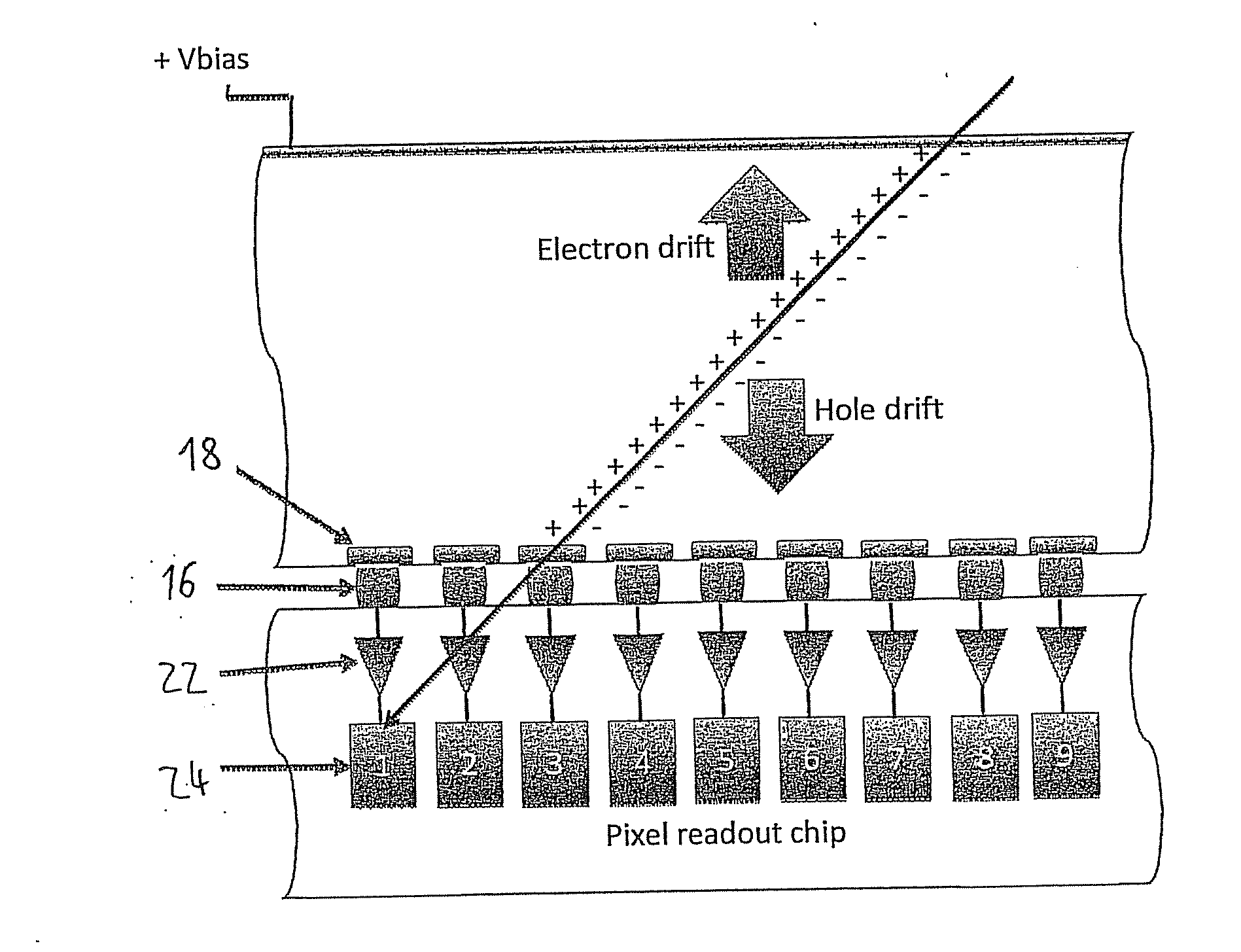
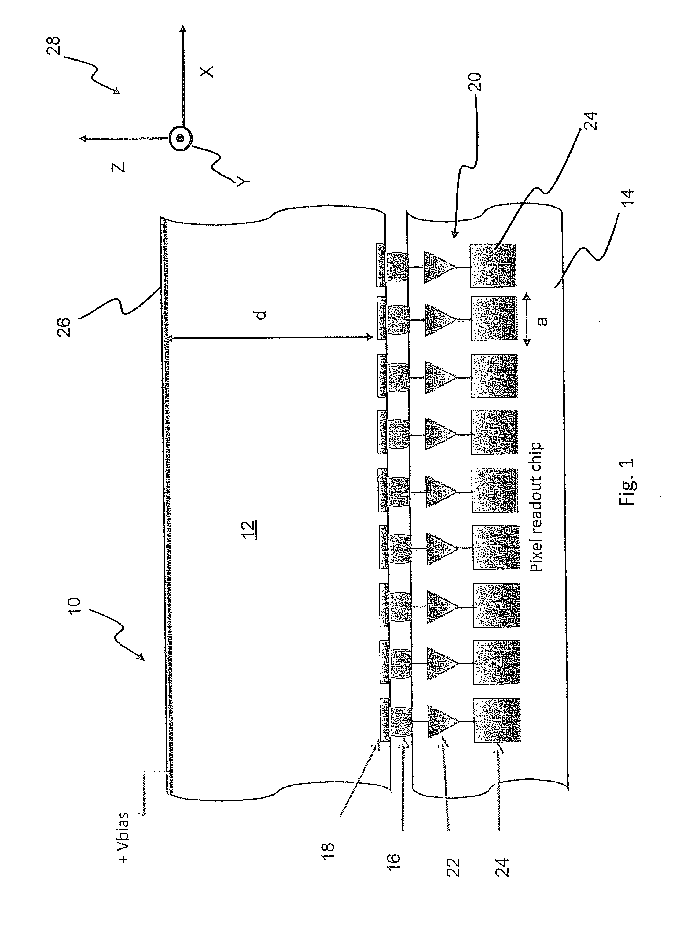
[0038]FIG. 1 is a sectional view of a pixel detector 10 according to an embodiment of the present invention. The pixel detector 10 comprises a semiconductor sensor layer 12, which in the present example is comprised of silicon. The pixel detector 10 further comprises a read-out electronics layer formed by a pixel read-out chip 14. The pixel read-out chip 14 is bon...


PUM


Abstract

The present invention relates to a pixel detector (10), comprising a semiconductor sensor layer (12), in which charges can be generated upon interaction with particles to be detected. The semiconductor layer defines an X-Y-plane and has a thickness extending in Z-direction. The detector further comprises a read-out electronics layer (14) connected to said semiconductor layer (12), said read-out electronics layer (14) comprising an array of read-out circuits (20) for detecting signals indicative of charges generated in a corresponding volume of said semiconductor sensor layer (12). The neighbouring read-out circuits (20) are connected by a relative timing circuit configured to determine time difference information between signals detected at said neighbouring read-out circuits (20). The time difference information is indicative of a difference in the Z-components of the locations of charge generations in the corresponding neighbouring sensor volumes caused by a particle trajectory that is inclined with respect to the X-Y-plane.

Description

FIELD OF THE INVENTION[0001]The present invention is in the field of particle detecting devices. Herein, the term “particle” refers to any type of radiation quanta, including photons. In particular, the present invention relates to a pixel detector comprising a semiconductor sensor layer and a read-out electronics layer to the semiconductor layer.DESCRIPTION OF THE RELATED ART[0002]Pixel detectors according to the preamble of claim 1 are known from prior art. The pixel detector of the preamble of claim 1 comprises a semiconductor sensor layer in which charges can be liberated upon interaction with particles to be detected. Ionizing radiation produces free electrons and holes in the semiconductor material. The number of electron-hole pairs generated is proportional to the energy transmitted by the particle to the semiconductor material. The detector further comprises a read-out electronics layer electrically connected to the semiconductor layer. For example, the read-out electronics ...

Claims


Application Information

Patent Timeline
IPC IPC(8): G01T1/29G01T1/24
CPCG01T1/2985G01T1/247G01T1/242G01T1/249H01L27/14661H01L31/085H01L31/115
Inventor CAMPBELL, MICHAELMICHEL, THILOJAKUBEK, JAN
Owner CZECH TECH UNIV IN PRAGUE
Why Eureka
Try Eureka