Imaging element

a technology of elements and elements, applied in the field of imaging elements, can solve the problems of increasing costs, reducing correspondingly increasing the amount of received light, so as to reduce the loss of process defects in the partition walls, improve the efficiency of light receiving, and reduce costs

Inactive Publication Date: 2014-11-27
FUJIFILM CORP
View PDF6 Cites 14 Cited by
  • Summary
  • Abstract
  • Description
  • Claims
  • Application Information

AI Technical Summary

Benefits of technology

[0009]The present invention has been developed in view of the foregoing circumstances. It is an object of the present invention to provide an imaging element in which light receiving efficiency is improved while suppressing cross talk of light which has passed through each color filter, without an increase in cost.
[0022]The imaging element of the present invention comprises the plurality of photoelectric converting elements that receive irradiation of light and convert the light into electrical charges; and the color filter layer which has a red filter, a green filter, and a blue filter which are respectively provided for each of the photoelectric converting elements. The partition walls having a lower refractive index than those of the red filter, the green filter, and the blue filter are provided only around the peripheries of the red filters. Therefore, light receiving efficiency can be improved compared to a case in which partition walls are provided at all of the boundaries among red filters, blue filters, and green filters.
[0023]In addition, process loss due to defects in the partition walls can be reduced, resulting in decreased costs.
[0024]In addition, the influence of cross talk caused by light entering red filters from green filters and blue filters is much greater than the influence of cross talk between green filters and blue filters, as will be described later. Therefore, the effect of suppressing cross talk can be sufficiently obtained, even if the partition walls are provided only around the peripheries of the red filters as in the imaging element of the present invention.
[0025]In addition, in the case that mask members that absorb or reflect the light are provided on the surfaces of the partition walls on the sides thereof that receive the light in the imaging element of the present invention, cross talk caused by light that enters the partition walls leaking into the red filters, the green filters, or the blue filters can be prevented.

Problems solved by technology

However, in imaging elements provided with partition walls at all of the boundaries among red filters, blue filters, and green filters as disclosed in Japanese Unexamined Patent Document No. 2009-111225, there is a problem that the amount of received light will decrease corresponding to the area occupied by the partition walls on the light receiving surface of the imaging elements.
Therefore, process loss due to defects in the partition walls will become likely to occur, resulting in increased costs.

Method used


Image

  • Imaging element
  • Imaging element
  • Imaging element

Examples


Embodiment Construction

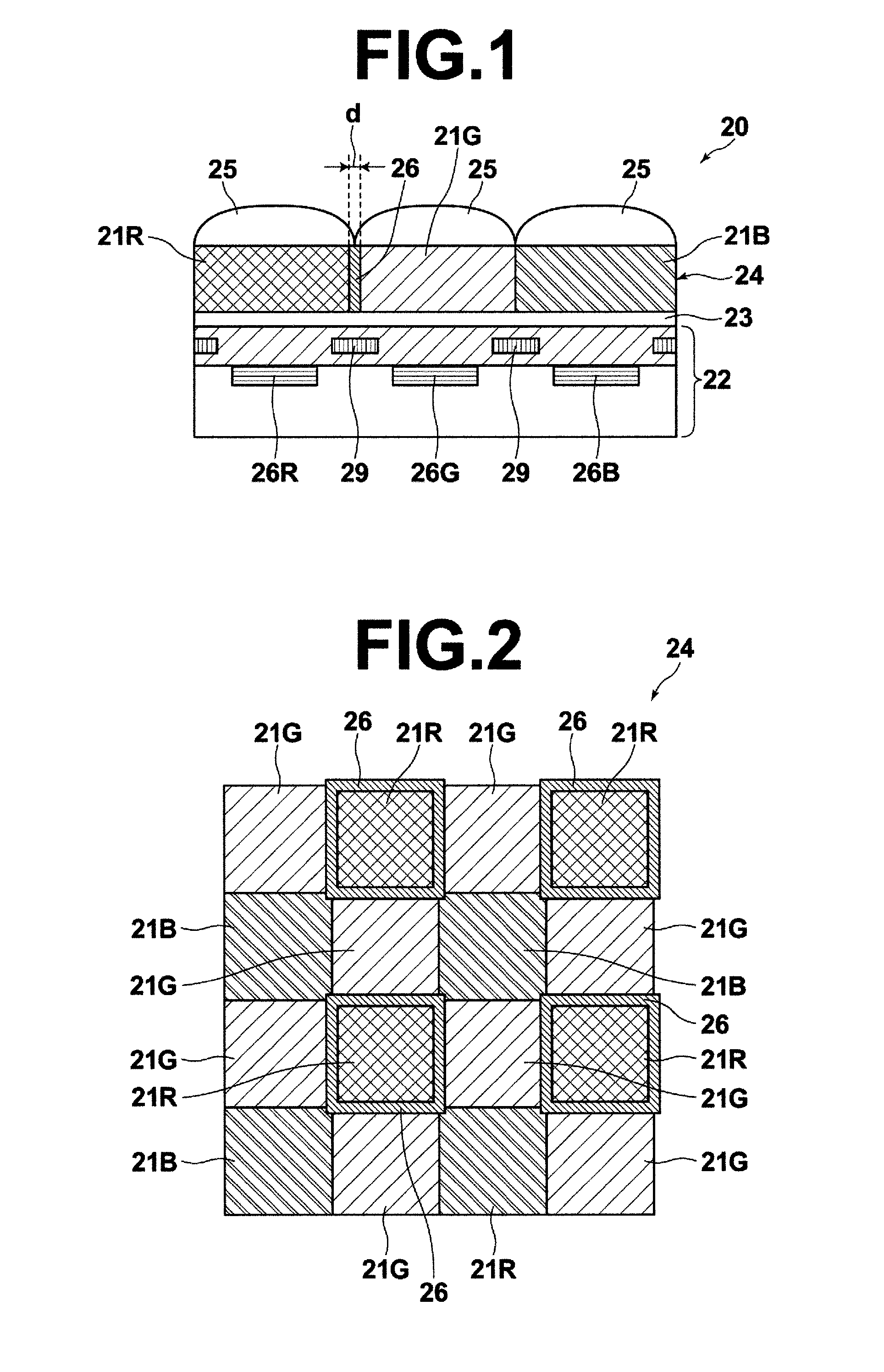
[0043]Hereinafter, an imaging element according to an embodiment of the present invention will be described in detail with reference to the attached drawings. FIG. 1 is a sectional diagram that schematically illustrates the configuration of the imaging element according to the embodiment of the present invention.

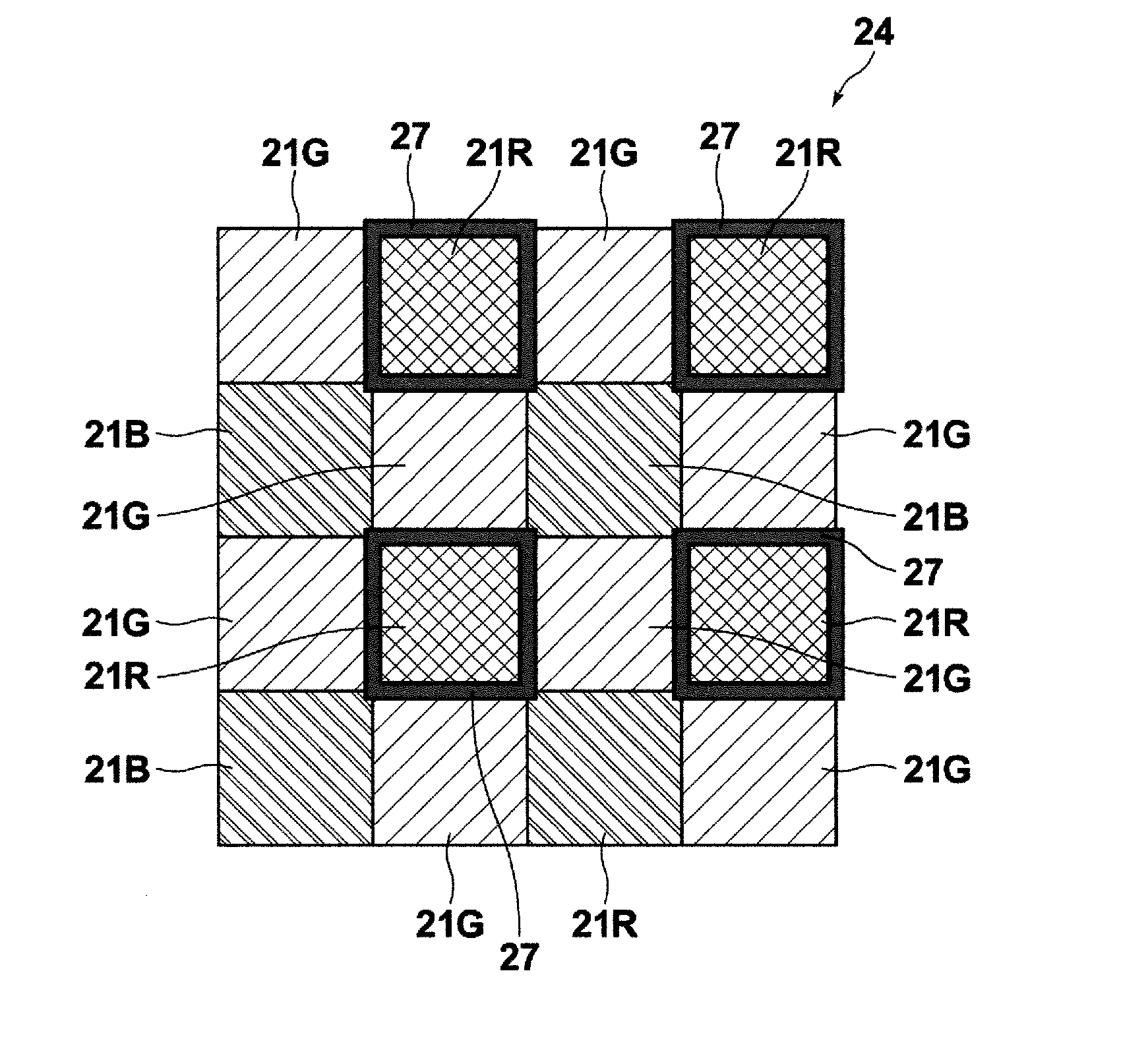
[0044]The imaging element 20 of the present embodiment is equipped with: a semiconductor substrate 22 having photodiodes (photoelectric converting elements) 26R, 26G, and 26B that generate electrical charges when irradiated with light; a device protecting film 23 formed on the semiconductor substrate 22; a color filter layer 24 having red filters 21R, green filters 21G, blue filters 21B, and partition walls 26 formed at the peripheries of the red filters 21R; and a microlens array 25 constituted by a great number of lenses provided to correspond to each of the red filters 21R, the green filters 21G, and the blue filters 21B, as illustrated in FIG. 1.

[0045]The imaging element...


PUM


Abstract

An imaging element includes: a plurality of photoelectric converting elements that receive irradiation of light and convert the light into electrical charges; and a color filter layer which has a red filter, a green filter, and a blue filter which are respectively provided for the photoelectric converting elements. Partition walls having a lower refractive index than those of the red filter, the green filter, and the blue filter are provided only around the peripheries of the red filters.

Description

CROSS REFERENCE TO RELATED APPLICATIONS[0001]The present application is a Continuation of PCT International Application No. PCT / JP2013 / 000658 filed on Feb. 7, 2013, which claims priority under 35 USC §119 (a) to Japanese Patent Application No. 2012-028329 filed on Feb. 13, 2012. Each of the above application(s) is hereby expressly incorporated by reference in its entirety, into the present application.TECHNICAL FIELD[0002]The present invention is related to an imaging element equipped with a color filter layer that has red filters, green filters, and blue filters.BACKGROUND ART[0003]Conventionally, various imaging elements such as CMOS's (Complementary Metal Oxide Semiconductors) and CCD's (Charge Coupled Devices), in which a plurality of photoelectric converting elements that convert light into electrical charges are arrayed, have been proposed.[0004]There are also known imaging elements provided with primary color filters, which are combinations of red filters, blue filters, and g...

Claims


Application Information

Patent Timeline
Patent Type & Authority Applications(United States)
IPC IPC(8): H01L27/146
CPCH01L27/14621H01L27/1463G02B5/201H01L27/14627H01L27/14685H01L27/14623H04N25/134H04N23/12
Inventor NAYA, MASAYUKITANI, TAKEHARU
Owner FUJIFILM CORP
Why Eureka
Try Eureka