
Semiconductor optical device assembly

a technology of semiconductor lasers and optical devices, applied in semiconductor lasers, electrical devices, laser details, etc., can solve the problems of affecting increasing the volume of light emitting layers, and affecting the device characteristics etc., to achieve the effect of reducing the reliability of quantum cascade lasers, dissipating heat generated in active layers, and easy to be affected by mounting process stress

Inactive Publication Date: 2014-11-27
SUMITOMO ELECTRIC IND LTD
View PDF4 Cites 11 Cited by
  • Summary
  • Abstract
  • Description
  • Claims
  • Application Information

AI Technical Summary

Benefits of technology

The patent describes a method to dissipate heat from a quantum cascade laser without causing stress and degradation in its performance. By using an electrode that extends over the entire laser and contacts the substrate, heat generated in the laser is transferred to the substrate through the electrode, which helps to cool the laser. This method prevents stress from being directly applied to the laser, improving its reliability and performance.

Problems solved by technology

Using such a long laser cavity leads to an increase in the volume of a light emitting layer.
However, when the quantum cascade laser is mounted on the sub-mount with its face down, a large stress tends to be generated in the active layer of the quantum cascade laser.
As a result, the degradation in device characteristics of the quantum cascade laser occurs.
Furthermore, the reliability of the quantum cascade laser also decreases due to the heat and stress in the active layer.

Method used


Image

  • Semiconductor optical device assembly
  • Semiconductor optical device assembly
  • Semiconductor optical device assembly

Examples


first embodiment

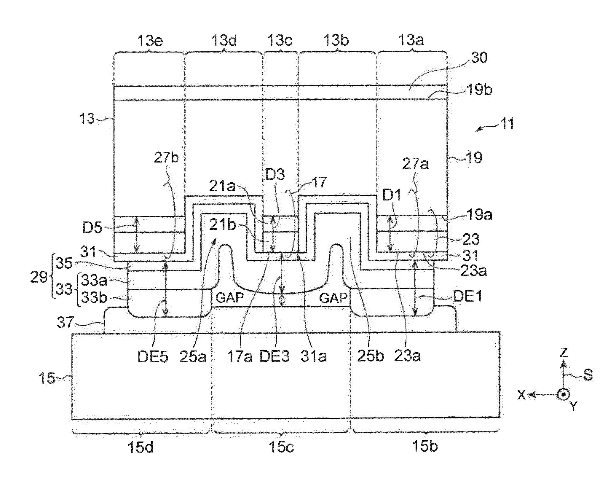
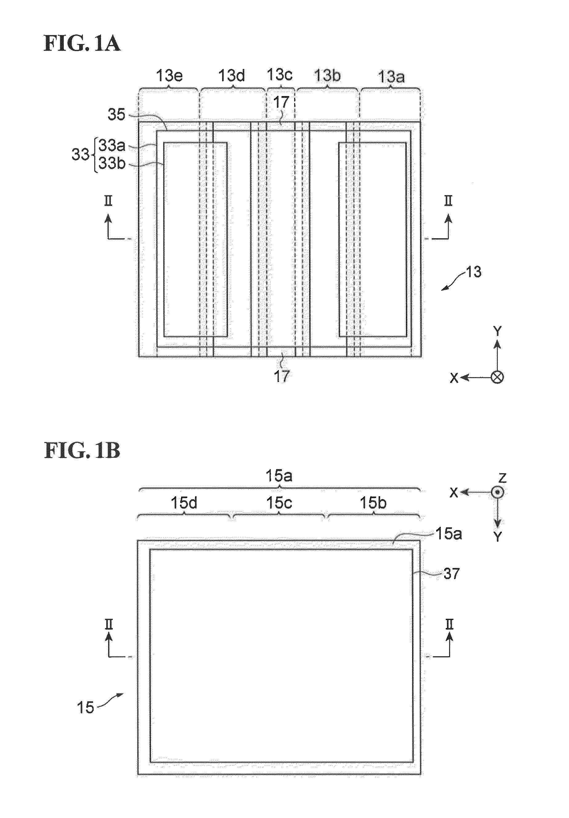
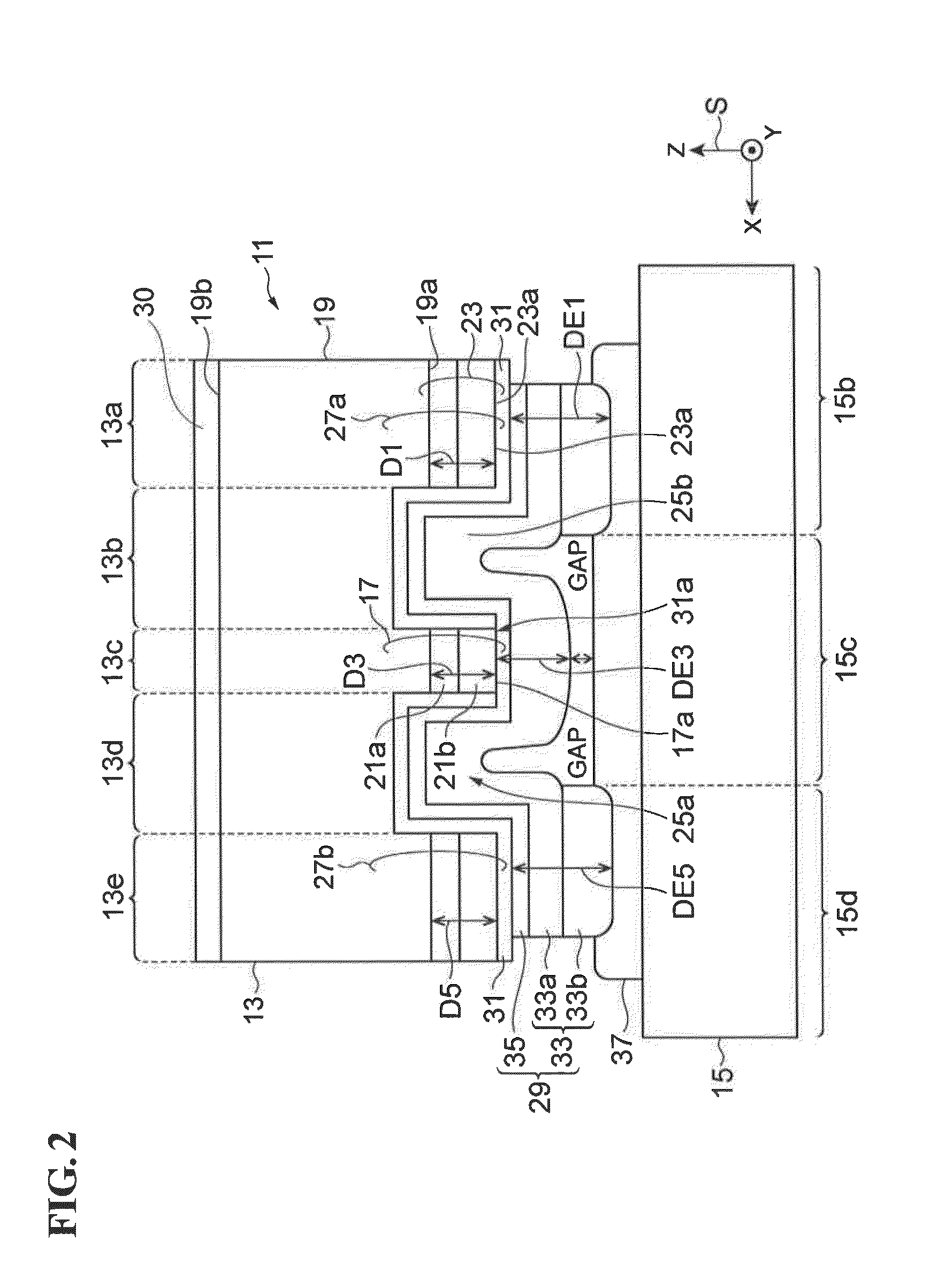
[0038]FIG. 1A is a plan view illustrating a quantum cascade laser. FIG. 1B is a plan view illustrating a sub-mount. FIG. 2 is a sectional view illustrating a semiconductor optical device assembly in which the quantum cascade laser illustrated in FIG. 1A is mounted on the sub-mount illustrated in FIG. 1B. FIG. 2 shows a sectional view taken along line II-II of FIGS. 1A and 1B. In each of FIGS. 1A, 1B, and 2, an orthogonal coordinate system S is shown to indicate the directions in the figure. A semiconductor optical device assembly 11 includes a quantum cascade laser 13 and a sub-mount 15. The sub-mount 15 has a mount surface 15a on which the quantum cascade laser 13 is mounted. The sub-mount 15 is made of a material that is different from a semiconductor. Therefore, the thermal expansion coefficient of the sub-mount 15 is different from the thermal expansion coefficient of the quantum cascade laser 13.

[0039]The quantum cascade laser 13 includes a first portion 13a, a second portion 1...

second embodiment

[0058]FIG. 3A is a plan view illustrating a quantum cascade laser. FIG. 3B is a plan view illustrating a sub-mount. FIG. 4 is a sectional view illustrating a semiconductor optical device assembly in which the quantum cascade laser illustrated in FIG. 3A is mounted on the sub-mount illustrated in FIG. 3B. FIG. 4 shows a sectional view taken along line IV-IV of FIGS. 3A and 3B. In each of FIGS. 3A, 3B, and 4, an orthogonal coordinate system S is shown to indicate the directions in the figure. A semiconductor optical device assembly 12 includes a quantum cascade laser 14 and a sub-mount 16. The sub-mount 16 has a mount surface 16a on which the quantum cascade laser 14 is mounted. The sub-mount 16 is made of a material that is different from a semiconductor. Therefore, the thermal expansion coefficient of the sub-mount 16 is different from the thermal expansion coefficient of the quantum cascade laser 14.

[0059]The quantum cascade laser 14 includes a first portion 14a, a second portion 1...


PUM


Abstract

A semiconductor optical device assembly includes a quantum cascade laser including first to fifth portions; and a sub-mount having a mount surface including first to third areas, the first area and the third area supporting the first portion and the fifth portion of the quantum cascade laser. The quantum cascade laser includes a substrate having a main surface; a semiconductor mesa disposed on the main surface in the third portion, the semiconductor mesa including a light emitting layer; and an electrode disposed on a surface in the first to fifth portions of quantum cascade laser, the electrode being in contact with an upper surface of the semiconductor mesa. The quantum cascade laser is mounted on the sub-mount with a gap formed between a surface of the electrode of the third portion of the quantum cascade laser and the second area of the sub-mount.

Description

BACKGROUND OF THE INVENTION[0001]1. Field of the Invention[0002]The present invention relates to a semiconductor optical device assembly.[0003]2. Description of the Related Art[0004]Japanese Unexamined Patent Application Publication No. 2003-332676 describes a semiconductor optical device having a structure that prevents damage to a waveguide region in a manufacturing process and a mounting process. The semiconductor optical device includes a waveguide region disposed between a pair of mesa grooves. A first mount region and a second mount region are disposed outside of the mesa grooves. A first spacer layer and a second spacer layer are respectively disposed in the first mount region and the second mount region. A first metal layer is electrically connected to an upper cladding layer of the waveguide region, and the first metal layer extends from an upper part of the waveguide region to an upper part of the first mount region. A second metal layer is disposed on an upper part of the...

Claims


Application Information

Patent Timeline
IPC IPC(8): H01S5/34H01S5/227H01S5/023H01S5/0233
CPCH01S5/227H01S5/3401H01S5/02461H01S5/02476H01S5/22H01S5/0234H01S5/023H01S5/0233H01S5/0235H01S5/0237
Inventor YOSHINAGA, HIROYUKIMURATA, MICHIO
Owner SUMITOMO ELECTRIC IND LTD
Learn More