Power module comprising two substrates and method of manufacturing the same

a technology of power modules and substrates, applied in the field of power modules, can solve the problems of high variation of the total thickness of the completed modules, and achieve the effects of reducing the thickness of the connecting layer, improving accuracy, and increasing manufacturing yield

Active Publication Date: 2014-12-04
INFINEON TECH AG
View PDF10 Cites 6 Cited by
  • Summary
  • Abstract
  • Description
  • Claims
  • Application Information

AI Technical Summary

Benefits of technology

[0010]The use of a compensation layer arranged between the two substrates may enable that thickness differences of the used substrates may be compensated for when arranging the two substrates in a stacked manner onto each other. In particular, tolerances or variations in the thickness of layers or elements of the module may be compensated for so that accuracy is improved, and / or a manufacturing yield may be increased. The use of a compensation layer may be advantageous, since additional processes or process steps may be omitted or avoided. Such additional processes or process steps in common manufacturing may relate to polishing or grinding used to reduce the thickness of a connecting layer or spacer connecting or contacting the two substrates of a module with each other. In particular, the compensation layer may function as a contacting or connecting layer as well. In particular, performing the thickness reduction after the second substrate is already arranged or disposed on the compensation layer may allow that thickness tolerances of the second substrate may be effectively compensated for by the compensation layer as well, which would be more difficult in case the compensation layer is polished or grinded to a specific thickness before the second substrate is arranged on the compensation layer.

Problems solved by technology

However, typical substrates used in power modules often have, due to the manufacturing process of the substrates, a rather high variation in thicknesses, which variation of the substrates' thicknesses leads to a rather high variation of the total thickness of the completed modules.

Method used


Image

  • Power module comprising two substrates and method of manufacturing the same
  • Power module comprising two substrates and method of manufacturing the same
  • Power module comprising two substrates and method of manufacturing the same

Examples


Embodiment Construction

[0018]In the following, further exemplary embodiments of the methods and of modules will be explained. It should be noted that embodiments described in the context of a method may also be combined with embodiments of the modules and vice versa.

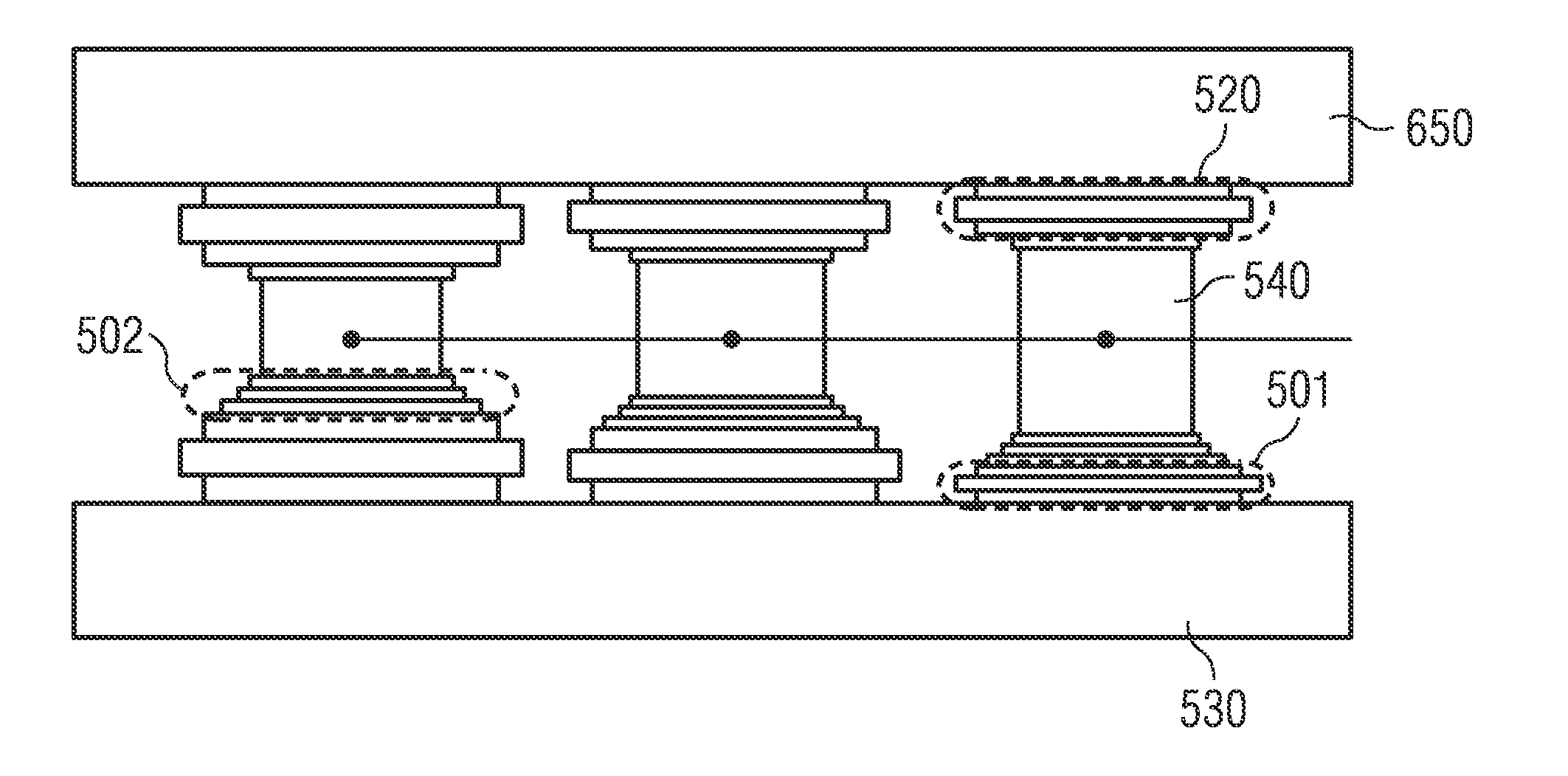
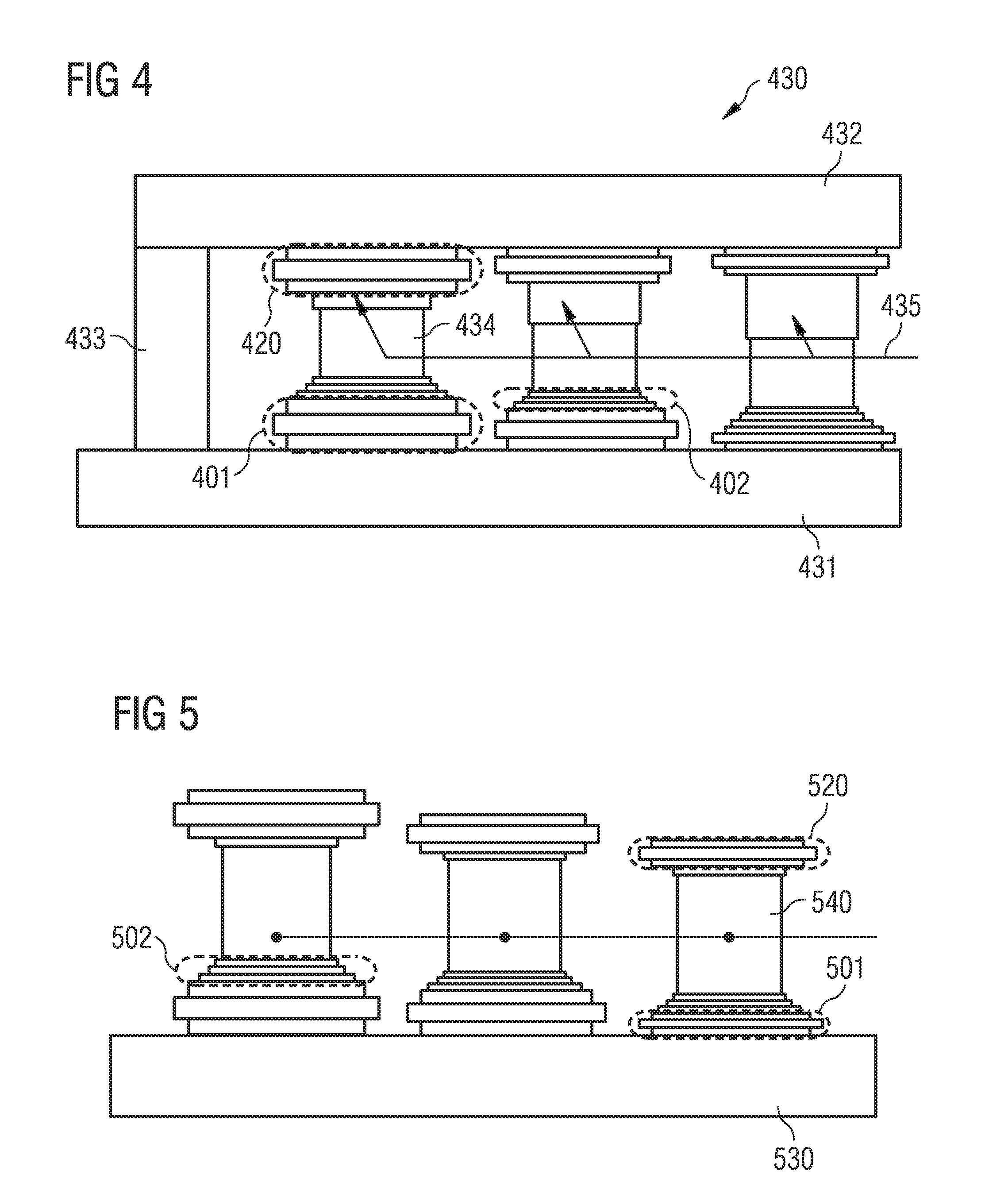
[0019]For example, the compensation layer may be a thickness compensation layer or in other words a layer adapted to compensate for thickness variations of layers or substrates arranged above or below the compensation layer. In particular, the first substrate may be a bottom substrate and / or the second substrate may be a top substrate. The thickness of the compensation layer or compensation structure may particularly be measured perpendicular with respect to main surfaces of the substrates and / or of the module. In particular, the reduction of the thickness of the compensation layer from the first thickness to a second thickness may be performed without grinding and / or without polishing and / or without abrasive processes. In particular, it shoul...


PUM


Abstract

A method of manufacturing a power module comprising two substrates is provided, wherein the method comprises disposing a compensation layer of a first thickness above a first substrate; disposing a second substrate above the compensation layer; and reducing the thickness of the compensation layer from the first thickness to a second thickness after the second substrate is disposed on the compensation layer

Description

BACKGROUND OF THE INVENTION[0001]1. Field of the Invention[0002]The present invention relates to power modules comprising two substrates and methods of manufacturing such modules.[0003]2. Description of the Related Art[0004]Conventional power modules comprising two substrates opposing each other are well known. In such modules the opposing two substrates often form the outer layers of the module. In order to enable a proper handling, processing and mounting in a larger module or device the dimensions, in particular the thickness, of the modules shall be as well defined as possible, i.e. a tolerance for the total thickness of the module shall be limited to a given threshold. However, typical substrates used in power modules often have, due to the manufacturing process of the substrates, a rather high variation in thicknesses, which variation of the substrates' thicknesses leads to a rather high variation of the total thickness of the completed modules.[0005]Thus, there is still poten...

Claims


Application Information

Patent Timeline
Patent Type & Authority Applications(United States)
IPC IPC(8): H01L21/56H01L23/00H01L23/31
CPCH01L21/56H01L24/89H01L23/31H01L23/3107H01L23/3735H01L23/49531H01L23/49575H01L23/4334H01L2924/13055H01L2924/1306H01L2924/1305H01L2924/00H01L2924/15787H01L2224/83139H01L2224/26135H01L24/29H01L24/32H01L24/83H01L24/97H01L25/50H01L2224/29005H01L2224/29124H01L2224/29147H01L2224/83048H01L2224/83191H01L2224/83201H01L2224/97H01L2224/30181H01L2924/181H01L2224/291H01L2224/2612H01L2224/83H01L2924/00012H01L2924/00014H01L2924/014
Inventor GEITNER, OTTMARHABLE, WOLFRAMGRASSMANN, ANDREASWINTER, FRANKNEUGIRG, CHRISTIANNIKITIN, IVAN
Owner INFINEON TECH AG
Why Eureka
Try Eureka