Method for manufacturing polysilicon

a manufacturing method and polysilicon technology, applied in the direction of crystal growth process, polycrystalline material growth, silicon compounds, etc., can solve the problems of excessive supply of raw material gas, reduced ratio of raw material gas contributing to deposition reaction, and increased deposition amount, so as to prevent meltdown, reduce the effect of energy consumption and reduce the effect of consumption

Active Publication Date: 2014-12-04
HANWHA CHEMICAL CORPORATION
View PDF2 Cites 0 Cited by
  • Summary
  • Abstract
  • Description
  • Claims
  • Application Information

AI Technical Summary

Benefits of technology

[0026]The method for manufacturing polysilicon according to the present invention can be used to prevent meltdown during the growth of silicon rod and to shortly manufacture a polycrystalline silicon rod having a diameter of 150 mm or larger with a minimal consumption of energy, and thus it is advantageous in terms of productivity and energy efficiency.

Problems solved by technology

However, it is not preferable that the raw material gas is excessively supplied, because a ratio of the raw material gas contributing to the deposition reaction is decreased to reduce a deposition amount (yield) of polycrystalline silicon.
Accordingly, when the rod grows to some extent and the temperature of the center portion of the rod reaches a melting point of polycrystalline silicon, meltdown is likely to easily occur.
Thus, there is a problem in that the rod cannot be grown to have a large diameter of, for example, 150 mm or larger.
However, the reaction yield is still lowered, and there is an inconvenience such as modification of the reactor structure.

Method used


Image

  • Method for manufacturing polysilicon
  • Method for manufacturing polysilicon

Examples


example 1

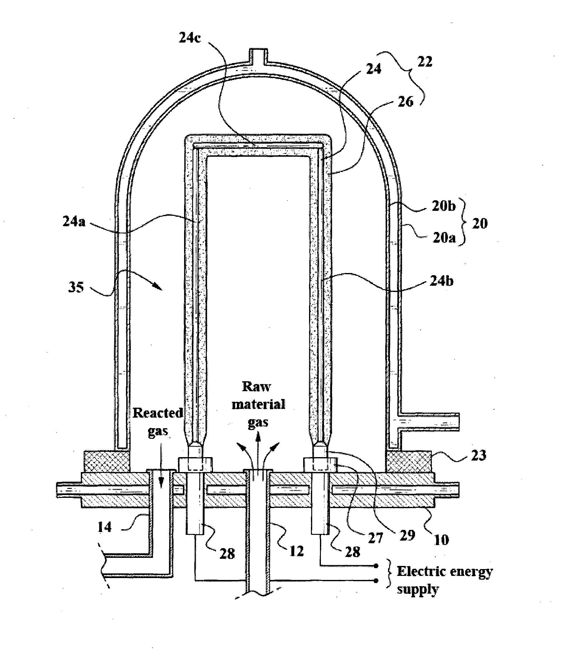
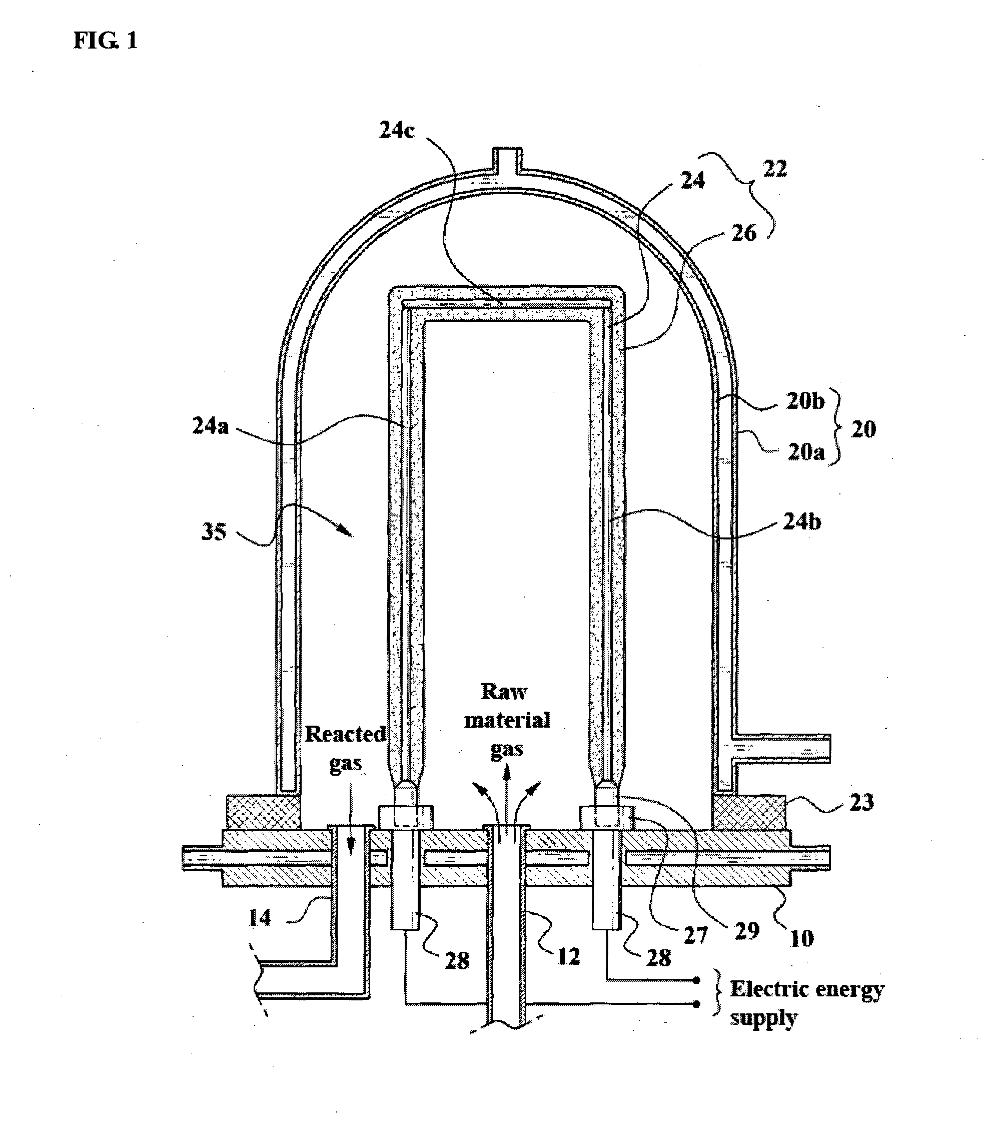
[0083]Polysilicon was produced using a reactor having a structure as shown in FIG. 1.

[0084]In this regard, the number of silicon rods (initial diameter of approximately 7 mm) installed inside the reactor was total 54, and the pressure inside the reactor was adjusted to approximately 6 bar absolute.

[0085]Dichlorosilane (DCS) and trichlorosilane (TCS) were contained in a raw material gas, and hydrogen gas (H2) was mixed with the raw material gas at a molar ratio of hydrogen gas (H2) to the raw material gas of approximately 1:8. The raw material gas was pre-heated to approximately 175° C., and a supply amount of the raw material gas per square millimeter of the surface of the silicon rod was approximately 2.0×10⁻⁷ (mol / sec / mm2).

[0086]The current value was set to maintain the average surface temperature of the silicon rod at approximately 1150° C. When the diameter of the silicon rod became approximately 150 mm, it was determined that the process was progressed to 100%, and the energy c...

example 2

[0090]Polysilicon was manufactured according to the reaction progress in the same manner and under the same conditions as in Example 1, except that until the process reached approximately 50%, the molar ratio of DCS to TCS contained in the raw material gas was adjusted to approximately 50 mol %, and then until the reaction was completed, the molar ratio of DCS to TCS contained in the raw material gas was adjusted to approximately 5 mol %.

example 3

[0091]Polysilicon was manufactured according to the reaction progress in the same manner and under the same conditions as in Example 1, except that until the process reached approximately 40%, the molar ratio of DCS to TCS contained in the raw material gas was adjusted to approximately 65 mol %, and then until the reaction was completed, the molar ratio of DCS to TCS contained in the raw material gas was adjusted to approximately 5 mol %.


PUM

PropertyMeasurementUnit
surface temperatureaaaaaaaaaa
diameteraaaaaaaaaa
diameteraaaaaaaaaa

Abstract

The present invention relates to a method for manufacturing polysilicon. According to the present invention, meltdown can be prevented during the growth of silicon rod, and a polycrystalline silicon rod having a larger diameter can be shortly manufactured with a minimal consumption of energy.

Description

TECHNICAL FIELD[0001]The present invention relates to a method for manufacturing polysilicon.BACKGROUND OF ART[0002]Polycrystalline silicon, commonly known as polysilicon, is used as a basic raw material for photovoltaic and semiconductor industries, and the demand for polysilicon is rapidly growing with recent development of the industries.[0003]The method of manufacturing polysilicon is represented by a silicon deposition process (or chemical vapor deposition) which produces a solid phase of polysilicon from a raw material, silane gas.[0004]According to the silicon deposition process, silicon fine particles are generated from the silane raw material gas through hydrogen reduction and thermal decomposition under a high-temperature circumstance, and the generated silicon fine particles are deposited in a form of polycrystalline on the surface of rods or particles. For example, a Siemens deposition method using a chemical vapor deposition reactor and a deposition method using a fluid...

Claims


Application Information

Patent Timeline
Patent Type & Authority Applications(United States)
IPC IPC(8): C01B33/035
CPCC01B33/035B01J19/24B01J2219/00135B01J2219/00186B01J2219/002B01J2219/00231C01B33/027C30B28/14
Inventor RYU, HYUN-CHEOLPARK, JEA SUNGLEE, DONG-HOKIM, EUN-JEONGAHN, GUI RYONGPARK, SUNG EUN
Owner HANWHA CHEMICAL CORPORATION
Why Eureka
Try Eureka