
Eureka
For R&D, Eureka makes reading and utilizing patents & technical documents easy.
Eureka AIR
Designed for self-driven R&D workflows. Generate viable solutions, solve complex R&D challenges, empower your innovation with AI.

Eureka Materials
Designed for material experts only. Revolutionize your material R&D, from search, analyze, to developing new materials.

TechResearch
Generate reliable direction feasibility study reports for your R&D in just a few steps.

TechSeek
Discover and master advanced knowledge NOW. Basics, ideas, possibilities, all at once.

TechMind
As an expert in R&D Theories, TechMind can generates customized viable solutions instantly.

TechRisk
Analyze your overall solution with one click, know your potential R&D risks in advance.

TechMonitor
Get weekly tech updates, stay abreast of the latest tech innovations and key insights.
Scanning electron microscope
- Summary
- Abstract
- Description
- Claims
- Application Information
AI Technical Summary
Benefits of technology
Problems solved by technology
Method used
Image

Examples
first embodiment
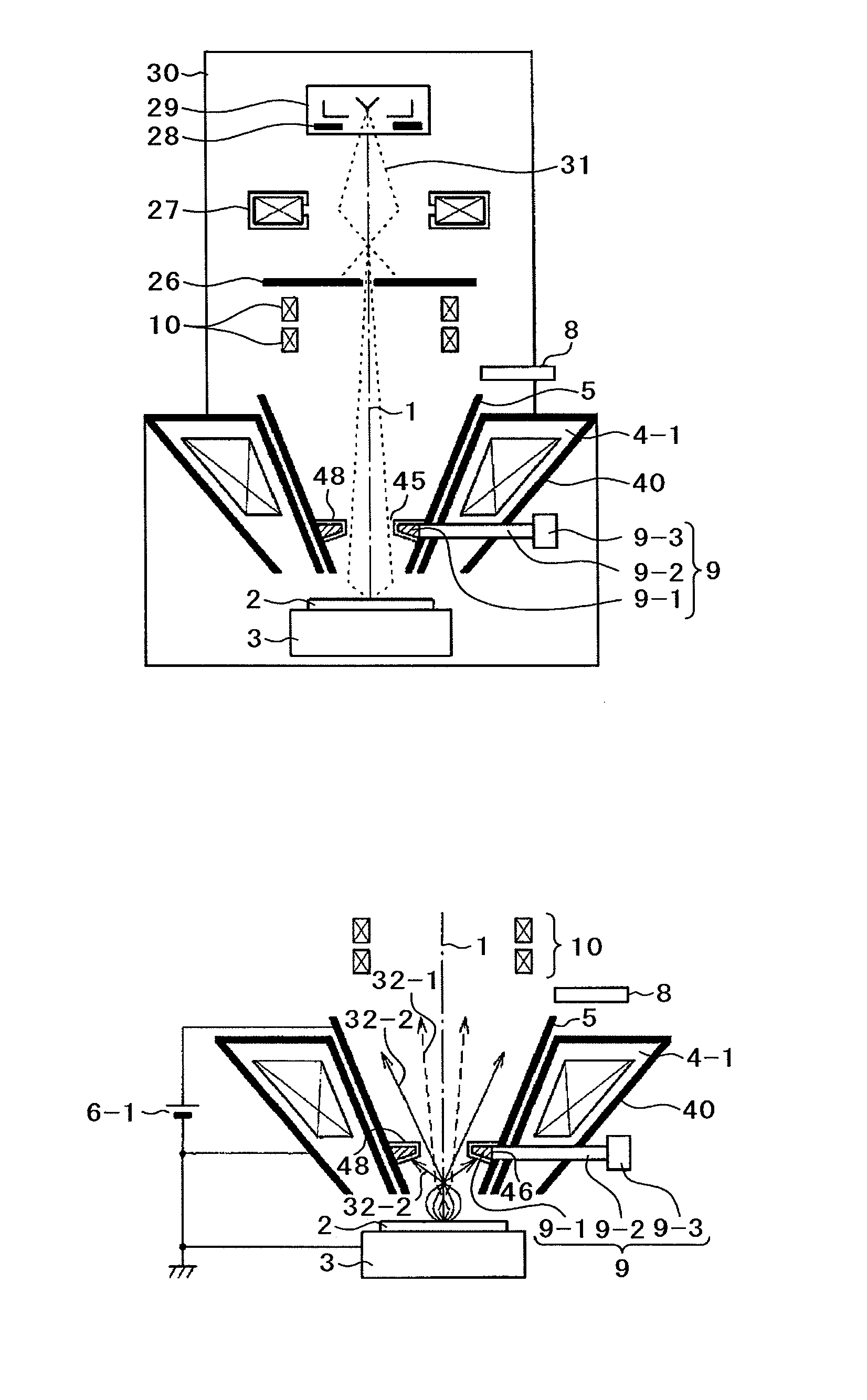
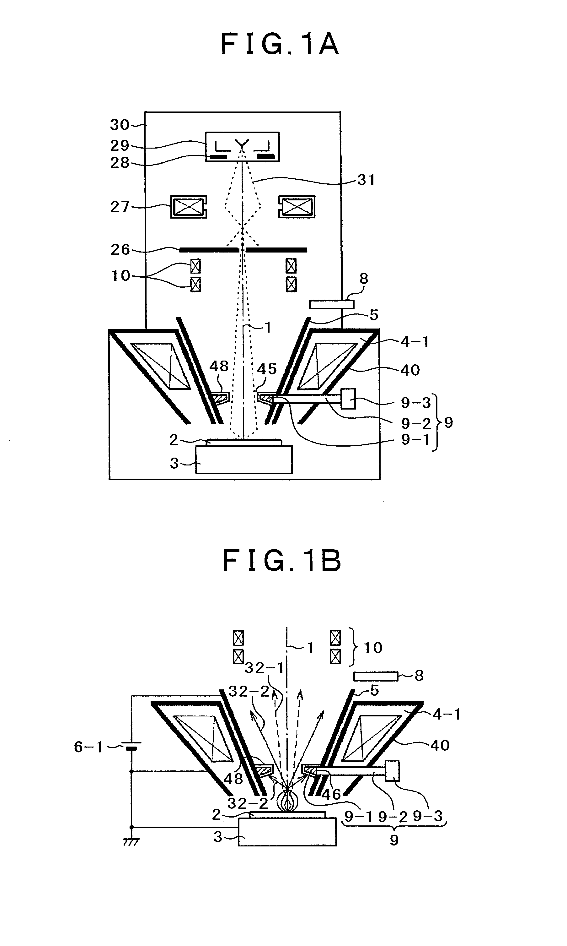
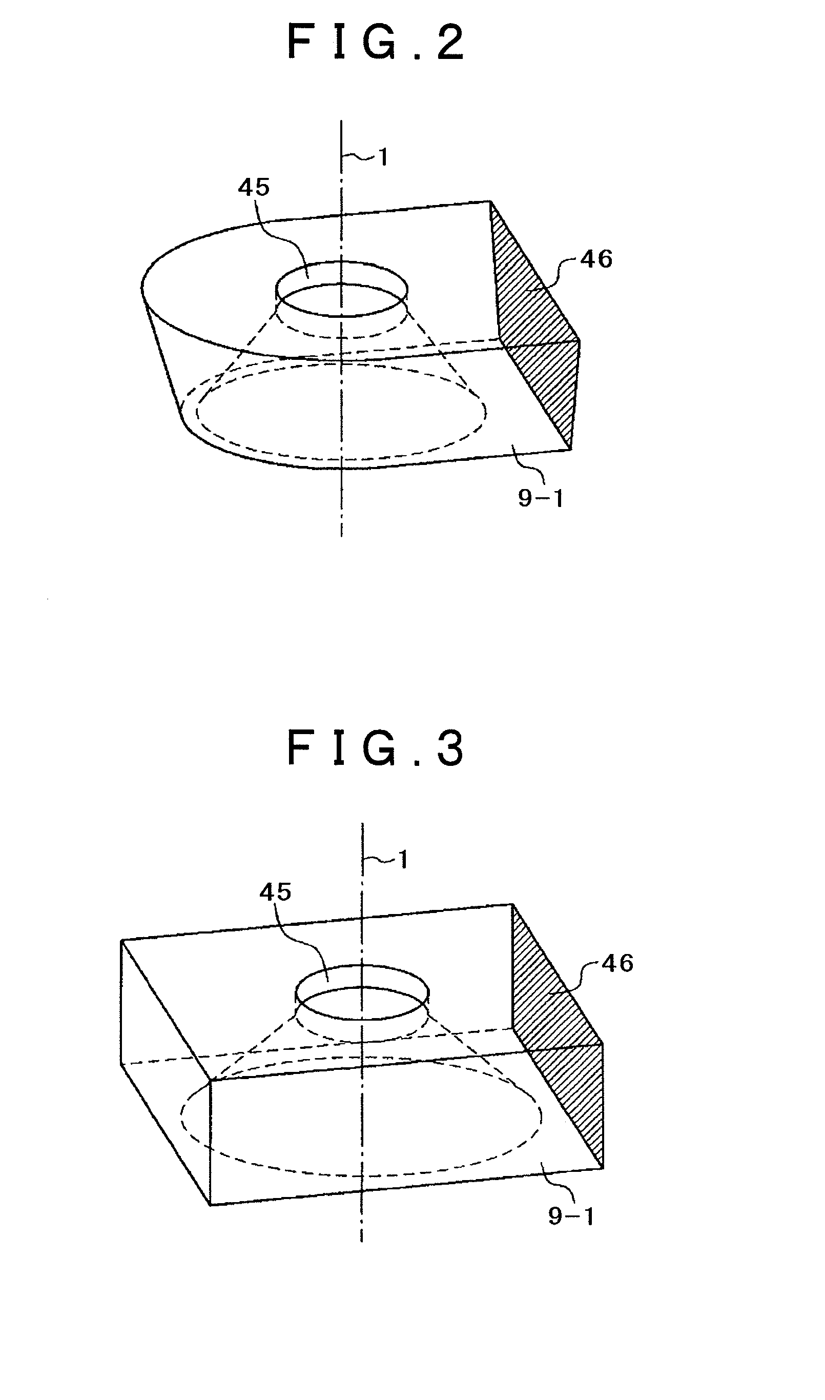
[0051]A first embodiment of the present invention will be explained with reference to FIGS. 1A, 1B, and 2 to 4. FIG. 1A is an entire schematic configuration diagram of the scanning electron microscope according to the embodiment. The scanning electron microscope shown in FIG. 1A is generally constituted by an electron optics column 30 equipped with a mechanism for emitting a primary electron beam 31 directed to a specimen 2, a specimen holder 3 holding the specimen 2, a specimen holder moving mechanism for placing and moving the specimen 2 to determine an observation region (not shown), a display device for an SEM image (not shown), a controller controlling the whole SEM (not shown), a vacuum exhaust installation (not shown), and the like.
[0052]The electron optics column 30 is basically constituted by an electron gun (electron source) 29, an acceleration electrode 28, at least one condenser lens 27, an aperture 26, an electron lens serving as an objective lens (shown herein is a sem...
second embodiment
[0069]A second embodiment will be explained with reference to FIGS. 5A to 5C. It should be noted that matters described in the first embodiment but not in this embodiment can be applied to this embodiment unless otherwise specified. FIG. 5A is a main part schematic cross-sectional view of a scanning electron microscope according to this embodiment.
[0070]This figure shows the components from the specimen holder 3 to the secondary electron detector 8 extracted from the system of the scanning electron microscope constituted by the electron gun 29, the acceleration electrode 28, the condenser lens 27, the aperture 26, the electron lens serving as the objective lens, the acceleration tube 5 for electrons, the deflector 10, the detector 8 for secondary electron detector 9 for backscattered electrons, the specimen holder 3 on which the specimen 2 is placed, the specimen holder moving mechanism for moving the specimen holder 3 to determine the observation region, the display device for an S...
third embodiment
[0079]A third embodiment will be explained with reference to FIGS. 6 to 15. It should be noted that matters described in the first or second embodiment but not in this embodiment can be applied to this embodiment unless otherwise specified. FIG. 6 is a main part schematic cross-sectional view of a scanning electron microscope according to this embodiment.
[0080]This figure shows the components from the specimen holder 3 to the secondary electron detector 8 extracted from the system of the scanning electron microscope constituted by the electron gun 29, the acceleration electrode 28, the condenser lens 27, the aperture 26, the electron lens serving as the objective lens, the acceleration tube 5 for electrons, the deflector 10, the detector 8 for secondary electron detector 9 for backscattered electrons, the specimen holder 3 on which the specimen 2 is placed, the specimen holder moving mechanism for moving the specimen holder 3 to determine the observation region, the display device f...
PUM
 Abstract
Description
Claims
Application Information
 - R&D Engineer
- R&D Manager
- IP Professional
- Industry Leading Data Capabilities
- Powerful AI technology
- Patent DNA Extraction
Browse by: Latest US Patents, China's latest patents, Technical Efficacy Thesaurus, Application Domain, Technology Topic, Popular Technical Reports.
© 2024 PatSnap. All rights reserved.Legal|Privacy policy|Modern Slavery Act Transparency Statement|Sitemap|About US| Contact US: help@patsnap.com