Electron beam system and electron beam measuring and observing method

a technology of electron beam and electron beam, which is applied in the direction of material analysis using wave/particle radiation, instruments, nuclear engineering, etc., can solve the problems of electron beam distortion or magnification distortion dependent on the direction of the tilt and height of the sample, the conventional method of compensating for off-axis aberration of electron lenses such as spherical aberration cannot achieve the precision necessary for stereo image measurement, and the effect of reducing aberration in an imag

Inactive Publication Date: 2005-07-28
KK TOPCON
View PDF3 Cites 33 Cited by
  • Summary
  • Abstract
  • Description
  • Claims
  • Application Information

AI Technical Summary

Benefits of technology

[0011] In a device constituted as described above, an electron beam device of the electron beam system includes the electron beam source 1, the electron optical system 2, the sample holder 3, the sample tilting section 5, and the electron beam detecting section 4. The first measuring section photographs a reference template in a specific tilt state by means of the electron beam detecting section 4, to find the shape or coordinate values of the reference template based on an acquired stereo image. The calibration data preparing section 30 compares the measurement results of the reference template by the first measuring section with known reference data on the reference template, to prepare calibration data for a stereo image photographed by the electron beam detecting section. The calibration section 40 performs a calibration based on the calibration data so as to reduce aberration in an image of the sample detected by the electron beam detecting section 4. The second measuring section finds the shape or coordinate values of the sample 9 based on the stereo image, photographed by the electron beam detecting section 4, of the sample 9 placed in a tilt state created by the sample tilting section 5 on the sample holder 3, where the sample 9 is calibrated by the calibration section 40. In this manner, three-dimensional image measurement of a sample can be performed with high precision, irrespective of the tilt angle and height of the sample, by adjusting an electron optical system of a scanning charged-particle beam device so as to be suitable for image measurement.
[0021] In order to achieve the object above, an electron beam measuring method according to the present invention uses, as shown for example in FIG. 4, an electron beam system including an electron optical system 2 for irradiating an electron beam 7 emitted from an electron beam source 1 on a sample 9, a sample holder 3 for holding the sample 9, a sample tilting section 5 for tilting the sample holder 3 and the irradiated electron beam 7 relative to each other so that a stereo image can be acquired, and an electron beam detecting section 4 for detecting an electron beam 7 outgoing from the sample 9, and has the following steps. That is, a computer is caused to perform: a first measuring step (S102, S104, S106) of finding a shape or coordinate values of the reference template held by the sample holder 3 based on a stereo image of the reference template photographed by the electron beam detecting section 4 while the reference template and the irradiated electron beam 7 are tilted relative to each other by the sample tilting section 5; a calibration data preparing step (S108) of comparing measurement results of the reference template in the first measuring step with known reference data on the reference template, to prepare calibration data for a stereo image photographed by the electron beam detecting section; a calibration step (S110) of performing a calibration based on the calibration data so as to reduce aberration in an image of the sample detected by the electron beam detecting section 4; a second measuring step (S112, S114, S116) of finding a shape or coordinate values of the sample 9 based on a stereo image, photographed by the electron beam detecting section 4, of the sample 9 placed in a tilt state made by the sample tilting section 5 on the sample holder 3, where the sample 9 is calibrated in the calibration step; and an image displaying step (S118) of displaying a stereo image of the sample 9 based on the electron beam detected by the electron beam detecting section 4.
[0035] According to the electron beam system of this invention, the calibration data preparing section compares the measurement results of the reference template by the first measuring section with known reference data on the reference template, to prepare calibration data for a stereo image photographed by the electron beam measuring device, and the calibration section performs a calibration based on the calibration data so as to reduce aberration in an image of the sample detected by the electron beam detecting section 4. Therefore, three-dimensional image measurement of a sample can be performed with high precision, irrespective of the tilt angle and height of the sample, by adjusting an electron optical system of a scanning charged-particle beam device so as to be suitable for image measurement.
[0036] Also, according to the electron beam system and the reference sample for an electron beam system of this invention, the tilt angle, magnification, and distortions involved with the electron optical system, for example, can be calculated and corrected, thereby rectifying a photographed image and allowing measurement of a sample with high precision.

Problems solved by technology

However, in measuring a sample such as a semiconductor chip or a silicone wafer, in particular, electron beam distortion or magnification distortion dependent on the directions of the tilt and height of the sample may be present.
Therefore, conventional methods for compensating for off-axis aberration of electron lenses such as spherical aberration cannot achieve the precision necessary for stereo image measurement.
Also, there may be electron beam distortion or magnification distortion dependent on the directions of the tilt and height of the sample.
In fine processing of semiconductor in recent years, the width of the patterns formed on a chip, for example, is as small as in the order of submicrons, and the margin of dimensional error acceptable in three-dimensional shape measurement has been increasingly limited as compared with the past.
Therefore, conventional methods for the approximate tilt angle value or magnification and for compensating off-axis aberration of electron lenses such as spherical aberration cannot achieve the precision necessary for stereo image measurement.

Method used


Image

  • Electron beam system and electron beam measuring and observing method
  • Electron beam system and electron beam measuring and observing method
  • Electron beam system and electron beam measuring and observing method

Examples


first embodiment

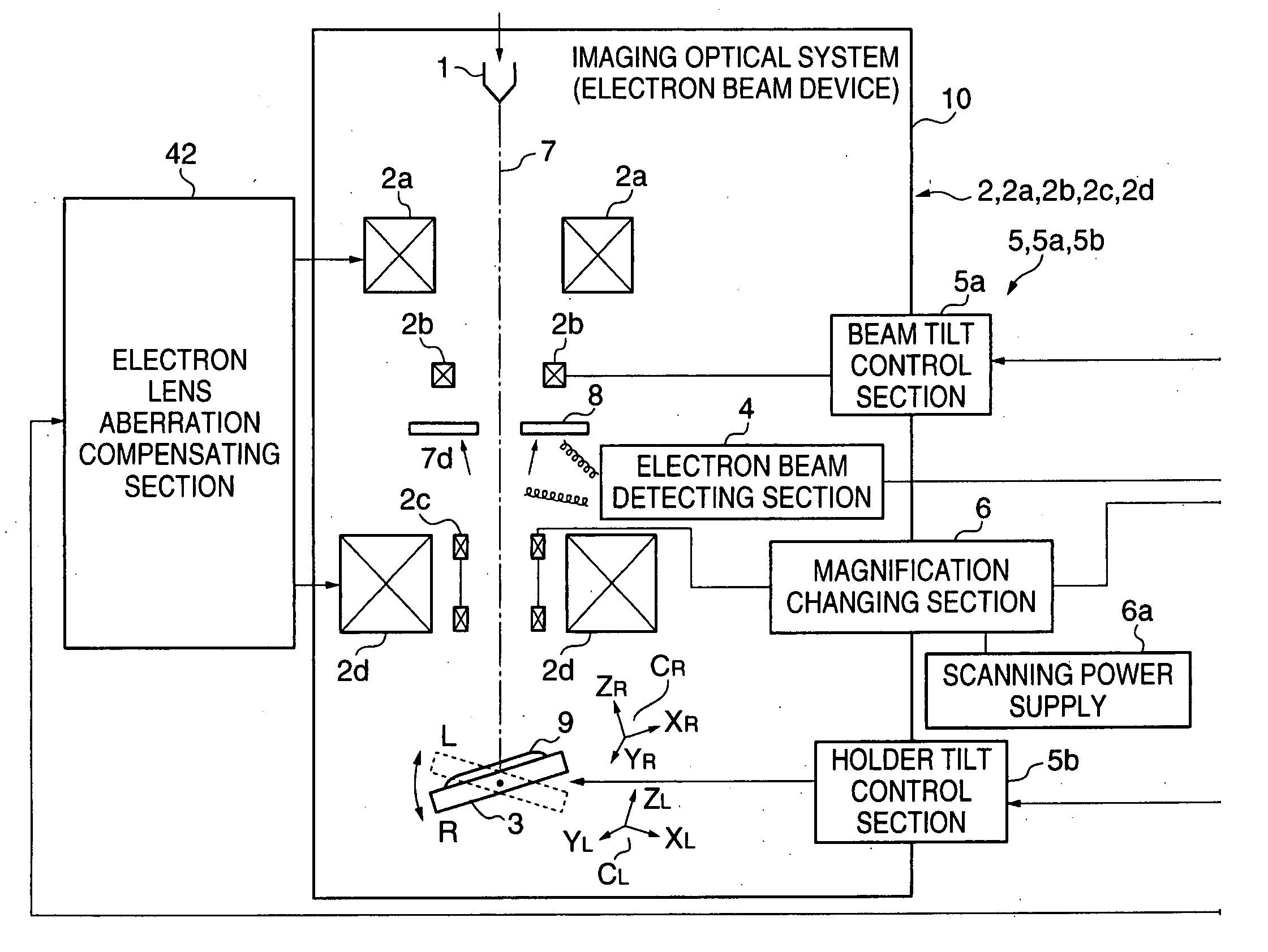
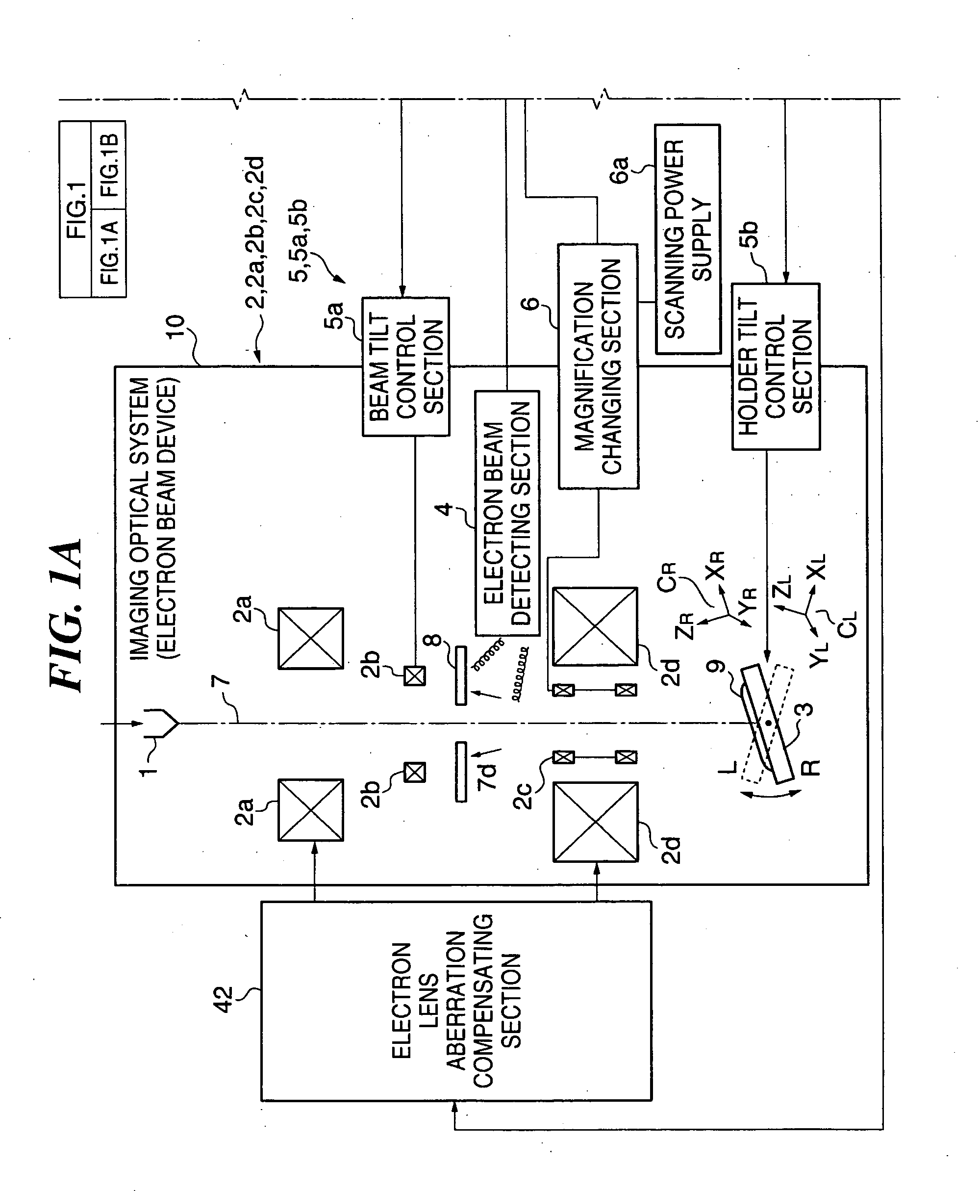
[0078] With reference to FIG. 1, an embodiment of this invention will be described hereinafter. FIG. 1 is a block diagram illustrating the structure of a first embodiment of this invention. In the first embodiment, the rotational angle of a holder for holding an object is adjusted to adjust the tilt angle of the object so that a stereo image of the object can be obtained. As shown in the figure, an electron beam device 10 (scanning electron microscope) as an imaging optical system in an electron beam measuring device as an electron beam system includes an electron beam source 1 for emitting an electron beam 7, an electron optical system 2 for irradiating the electron beam 7 on an object 9, a sample holder 3 for tiltably holding the object 9, a magnification changing section 6 for changing the magnification of the electron optical system 2, a scanning power supply 6a for supplying electric power to the magnification changing section 6, a detector 4 for detecting the electron beam 7, ...

second embodiment

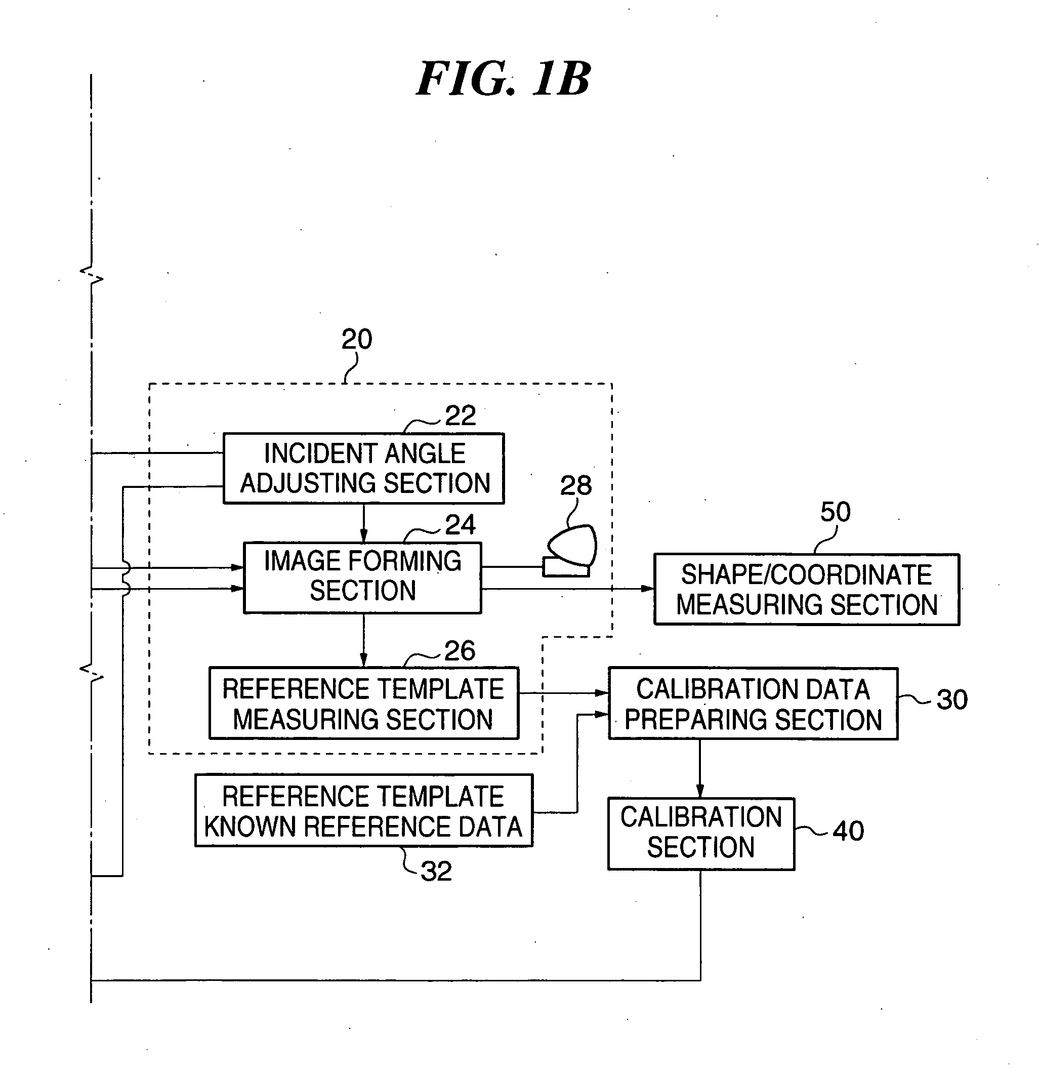
[0108]FIG. 6 is a block diagram illustrating the structure of a second embodiment of this invention. As shown in the figure, the electron beam measuring device includes an image correcting section 60, an image correction factor calculating section 62, and a correction factor storing section 64, in addition to the measuring section 20, the calibration data preparing section 30, the known reference data storing section 32, the calibration section 40, the electron lens aberration compensating section 42, and the shape / coordinate measuring section 50 described above.

[0109] The shape / coordinate measuring section 50 includes an approximate measurement section 52 and a precise measurement section 54. The approximate measurement section 52 finds the approximate shape or coordinate values of the sample 9 photographed in a stereo image. The precise measurement section 54 finds the shape or coordinate values of the sample 9 based on the stereo image corrected by the image correcting section 6...

third embodiment

[0142]FIG. 16 is a general block diagram illustrating the structure of a third embodiment of this invention. In the third embodiment, the electron beam of the scanning electron microscope 10a is deflected to obtain a stereo image, unlike the first and second embodiments, where the holder is tilted to obtain a stereo image. In FIG. 16, components corresponding to those in FIG. 1 are given the same reference numerals and symbols, and descriptions of them are not repeated. A beam tilt control section 5a for controlling the tilt of the electron beam 7 is provided as the tilt control section 5. The beam tilt control section 5a transmits a tilt control signal to the deflection lenses 2b so that the irradiated electron beam 7 is switched between an electron beam 7R which makes a first tilt angle relative to the sample holder 3 and an electron beam 7L which makes a second tilt angle relative to the sample holder 3. The beam tilt control section 5a may be able to adjust the relative tilt ang...


PUM

PropertyMeasurementUnit
tilt angleaaaaaaaaaa
shapeaaaaaaaaaa
electron beamaaaaaaaaaa

Abstract

This invention provides an electron beam measuring device capable of performing three-dimensional image measurement of a sample with high precision, irrespective of the tilt angle and height of the sample, by adjusting an electron optical system of a scanning charged-particle beam device so as to be suitable for image measurement. The electron beam measuring device includes a measuring section 20 adapted to tilt a reference template held by a sample holder 3 and an irradiated electron beam 7 relative to each other by means of a sample tilting section 5, to find the shape or coordinate values of the reference template based on a stereo image photographed by an electron beam detecting section 4, a calibration data preparing section 30 for comparing the measuring results at the measuring section 20 with known reference data to prepare calibration data for a stereo image photographed by the electron beam measuring device, and a calibration section 40 for performing a calibration based on the calibration data so as to reduce aberration in an image of the sample detected by the electron beam detecting section 4. Based on the stereo image calibrated by the calibration section 40, the shape or coordinate values of the sample 9 are found.

Description

BACKGROUND OF THE INVENTION [0001] 1. Technical Field [0002] This invention relates to an electron beam system and an electron beam measuring method capable of performing three-dimensional measurement of a sample with high precision, using a photographed sample image, and in particular to improvement in adjusting corrections made to an electron optical system of a scanning charged-particle beam device so as to be suitable for image measurement. [0003] This invention relates to an electron beam system and a reference sample for an electron beam system capable of performing three-dimensional measurement of a sample with high precision, using a photographed sample image, and in particular to an electron beam system and a reference sample for an electron beam system capable of adjusting, when the beam or sample of a scanning charged-particle beam device is tilted, corrections made to the angle and magnification and corrections made to an electron optical system, at the time of 3D measur...

Claims


Application Information

Patent Timeline
Patent Type & Authority Applications(United States)
IPC IPC(8): G01B15/00G01N23/00G01N23/225G06T7/00G21K7/00H01J37/28
CPCG01B15/00G01N23/2251G06T7/002H01J2237/2826H01J37/28H01J2237/2611H01J2237/2814G06T7/0075G06T7/593G06T7/85
Inventor KOCHI, NOBUOAOKI, HIROYUKI
Owner KK TOPCON
Why Eureka
Try Eureka