High-accuracy OLED touch display panel structure

a touch display panel and high-accuracy technology, applied in thermoelectric devices, instruments, solid-state devices, etc., can solve the problems of increasing the additional weight and thickness increasing the reflectance and haze of the touch display panel, and reducing the light penetration rate. , to achieve the effect of increasing the sensing linearity and sensing accuracy, reducing the gap distance between sensing touch patterns, and reducing the measurement of dead area

Active Publication Date: 2014-12-11
SUPERC TOUCH CORP
View PDF0 Cites 8 Cited by
  • Summary
  • Abstract
  • Description
  • Claims
  • Application Information

AI Technical Summary

Benefits of technology

[0013]The object of the present invention is to provide a high-accuracy OLED touch display panel structure, in which a plurality of wiring segments arranged in the first direction and a plurality of wiring segments arranged in the second direction are formed on a thin film transistor and wiring layer, such that there is no need to arrange wirings on a sensing electrode layer for the sensing touch pattern structure on the sensing electrode layer, so as to effectively reduce the gap distance between sensing touch patterns thereby decreasing the measure of dead area and increasing sensing linearity and sensing accuracy.

Problems solved by technology

Such well known skill of the touch panel may increase additional weight and thickness of the touch display panel, and may further reduce the light penetration rate, and increase reflectance and haze of the touch display panel.
Such a structure suffers the disadvantages of high material cost and complicated manufacturing process.
The structure of FIG. 4 has the advantages of low material cost and simplified manufacturing process; however, it suffers the disadvantage of complicated wirings 41.
Because the wirings 41 occupy most of the area, the linearity becomes unsatisfactory.

Method used


Image

  • High-accuracy OLED touch display panel structure
  • High-accuracy OLED touch display panel structure
  • High-accuracy OLED touch display panel structure

Examples


Embodiment Construction

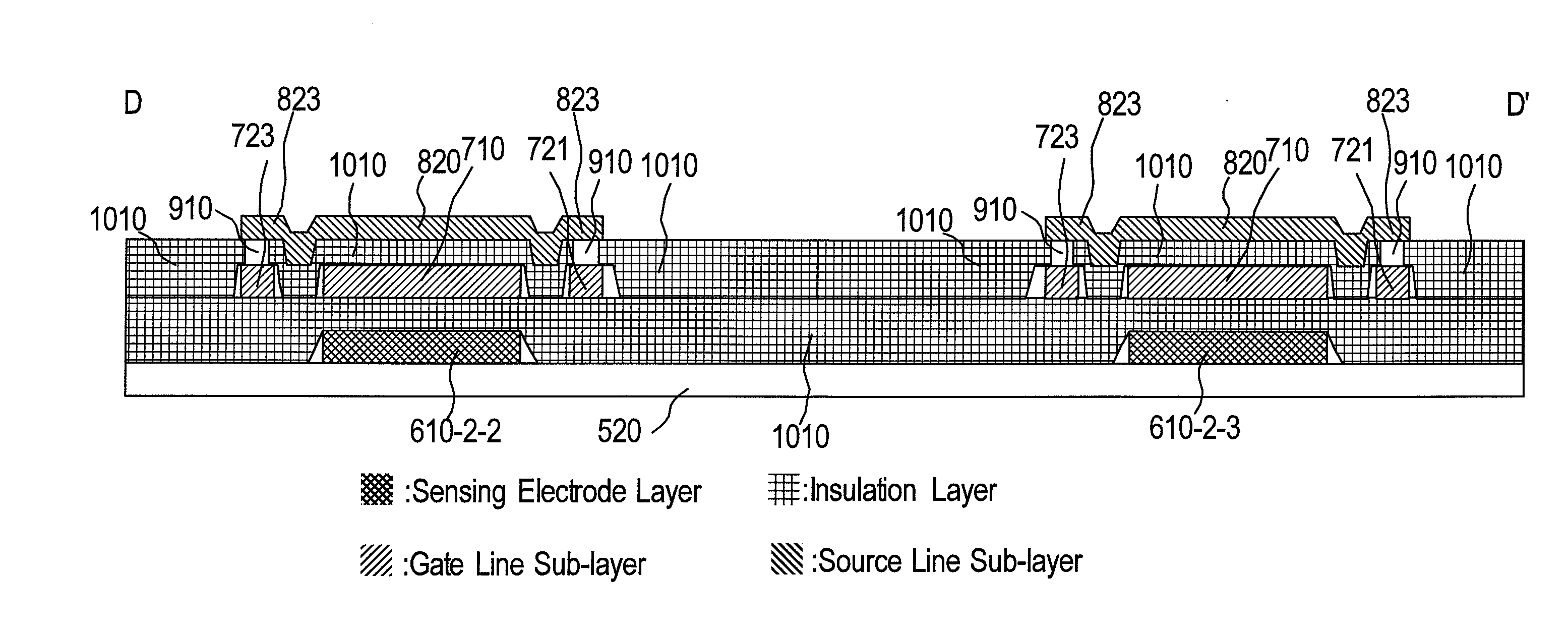
[0030]The present invention relates to a high-accuracy OLED touch display panel structure. FIG. 5 is a cross sectional view of the high-accuracy OLED touch display panel structure 500 in accordance with the present invention. The high-accuracy OLED touch display panel structure 500 includes an upper substrate 510, a lower substrate 520, a sensing electrode layer 530, an OLED layer 540, a thin film transistor and wiring layer 550, a cathode layer 560, and an anode layer 570.

[0031]The upper substrate 510 and the lower substrate 520 are preferably glass substrates or plastic substrates, and are parallel to each other. The OLED layer 540 is disposed between the upper and lower substrates 510, 520.

[0032]The sensing electrode layer 530 is disposed at one side of the lower substrate 520 that faces the OLED layer 540. The sensing electrode layer 530 has a plurality of sensing conductor lines for sensing an approaching external object.

[0033]The thin film transistor and wiring layer 550 is di...


PUM


Abstract

A high-accuracy OLED touch display panel structure includes an upper substrate, a lower substrate, an OLED layer configured between the upper and lower substrates, a sensing electrode layer, a thin film transistor and wiring layer, a cathode layer, and an anode layer. The sensing electrode layer has a plurality of sensing conductor lines for sensing an approaching external object. The thin film transistor and wiring layer includes a plurality of gate lines, a plurality of source lines, and a plurality of wirings. The plurality of sensing conductor lines are disposed corresponding to positions of the plurality of gate lines and the plurality of source lines.

Description

BACKGROUND OF THE INVENTION[0001]1. Field of the Invention[0002]The present invention relates to a structure of touch display panel and, more particularly, to a high-accuracy OLED touch display panel structure.[0003]2. Description of Related Art[0004]In recent year, the flat panel display industry has been rapidly developed, and many products have also been made in pursuit of light weight, thinness, small volume and fine image quality for developing several types of flat-panel displays to replace traditional cathode ray tube display (CRT). FIG. 1 schematically illustrates the types of known display panels. As shown in FIG. 1, the flat panel display includes liquid crystal display (LCD), plasma display panel (PDP), organic light emitting diode (OLED) display, field emission display (FED), and vacuum fluorescence display (VFD).[0005]Among these types of flat panel displays, the organic light emitting diode display (OLED) technology is the one with great potential. OLED was first publi...

Claims


Application Information

Patent Timeline
Patent Type & Authority Applications(United States)
IPC IPC(8): H01L27/32G06F3/041G06F3/047
CPCH01L27/323G06F3/0412G06F3/047G06F2203/04111G06F3/0443H10K59/40
Inventor LEE, HSIANG-YU
Owner SUPERC TOUCH CORP
Why Eureka
Try Eureka