Semiconductor light-emitting diode and method for manufacturing the same

a technology of semiconductor led and light-emitting diodes, which is applied in the direction of semiconductor/solid-state device manufacturing, semiconductor devices, electrical apparatus, etc., can solve the problems of difficult to create efficient hole injection, impeding the improvement of quantum efficiency of semiconductor led, and high hole concentration, so as to improve the quantum efficiency of led and improve the efficiency of hole injection

Active Publication Date: 2014-12-25
HC SEMITEK CORP
View PDF2 Cites 13 Cited by
  • Summary
  • Abstract
  • Description
  • Claims
  • Application Information

AI Technical Summary

Benefits of technology

[0020]Advantages according to embodiments of the invention are summarized below. The embodiments of the present invention design and optimize the changes of the Al component of the electron blocking layer by energy band engineering, namely by arranging the first and second AlGaN layers which are alternately stacked and form a structure like a superlattice structure to generate a three-dimensional free hole gas in the p-GaN layer and, in turn, obtain a high hole concentration which can reach an order of 1*e18 cm−3. Then the overflow of the electrons can be blocked, while hole injection efficiency can be improved, thereby improving the quantum efficiency of the LED.

Problems solved by technology

It inhibits the leakage of the electron at the expense of hole injection efficiency.
It is difficult to create an efficient hole injection under forward bias, thereby impeding the improvement of the quantum efficiency of the semiconductor LED.

Method used


Image

  • Semiconductor light-emitting diode and method for manufacturing the same
  • Semiconductor light-emitting diode and method for manufacturing the same
  • Semiconductor light-emitting diode and method for manufacturing the same

Examples


example 1

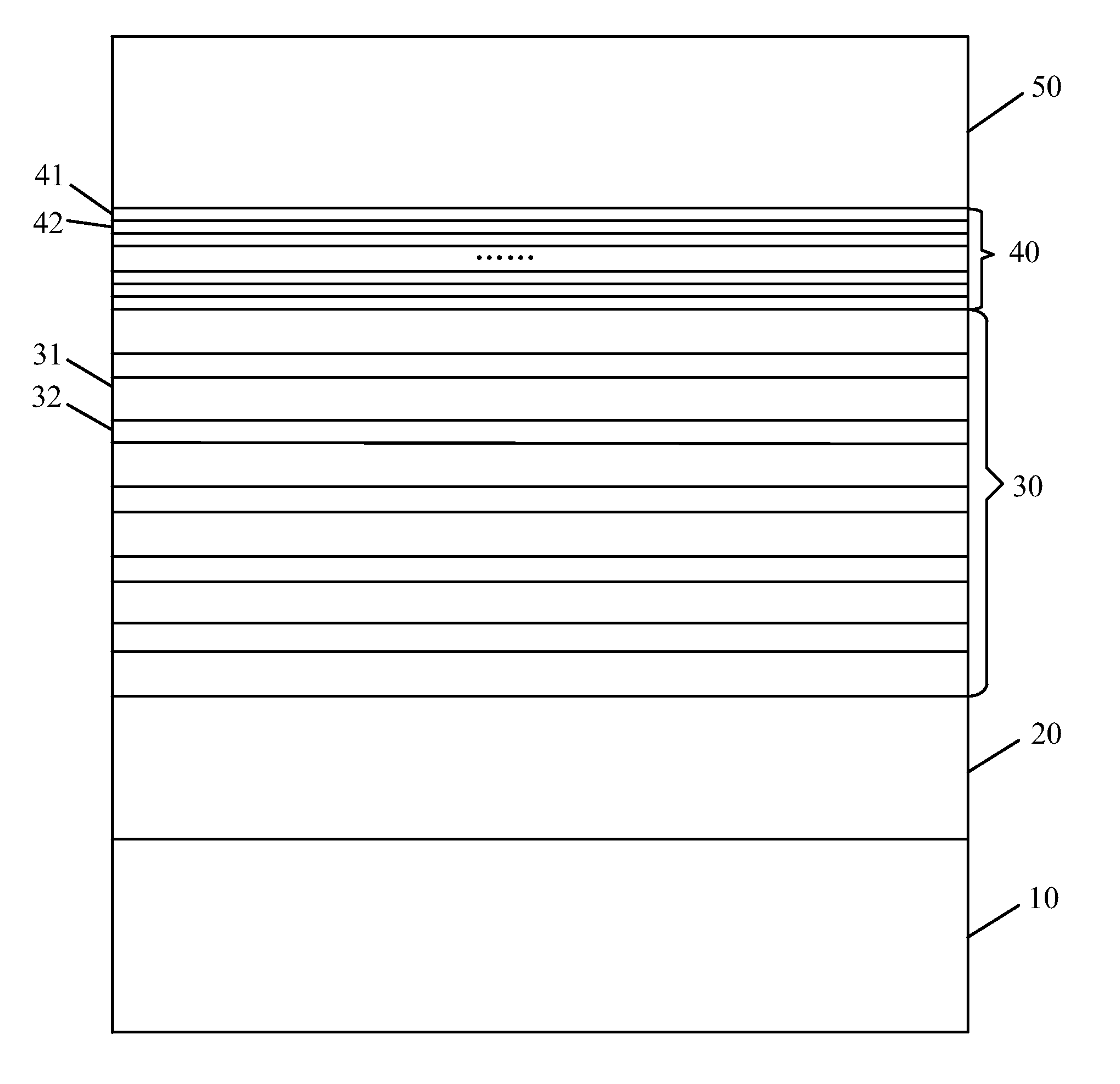
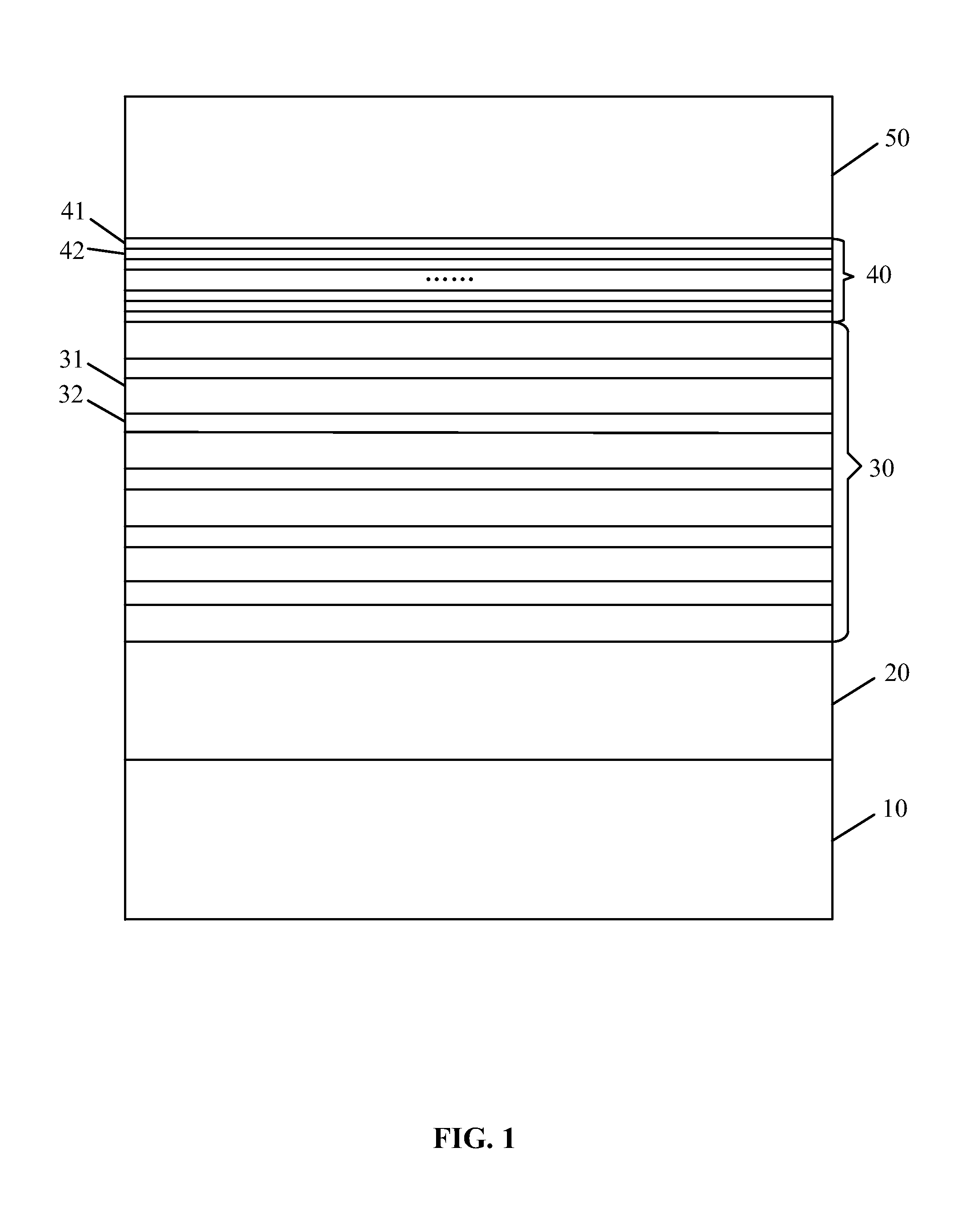
[0043]The semiconductor LED in Example 1 has the same structure as the abovementioned example. In this example, the distribution of Al component of the first AlGaN layers and the second AlGaN layers of the electron blocking layer is shown in FIG. 2. In FIG. 2, white boxes represent the first AlGaN layers, black boxes represent the second AlGaN layers, and the height of the boxes indicates the size of the content of the layer of Al components. A left side of the figure denotes the side of the quantum well layer, and a right side of the figure denotes the side of the p-GaN layer.

[0044]As shown in FIG. 2, in this example, from the side of the quantum well layer to the side of the p-GaN layer, namely from the left side to the right side, the Al component of the plurality of first AlGaN layers 41 is gradually increased layer by layer, and the Al component of the plurality of second AlGaN layers 42 are invariable.

[0045]In this example, the electron blocking layer 40 may comprise, but not ...

example 2

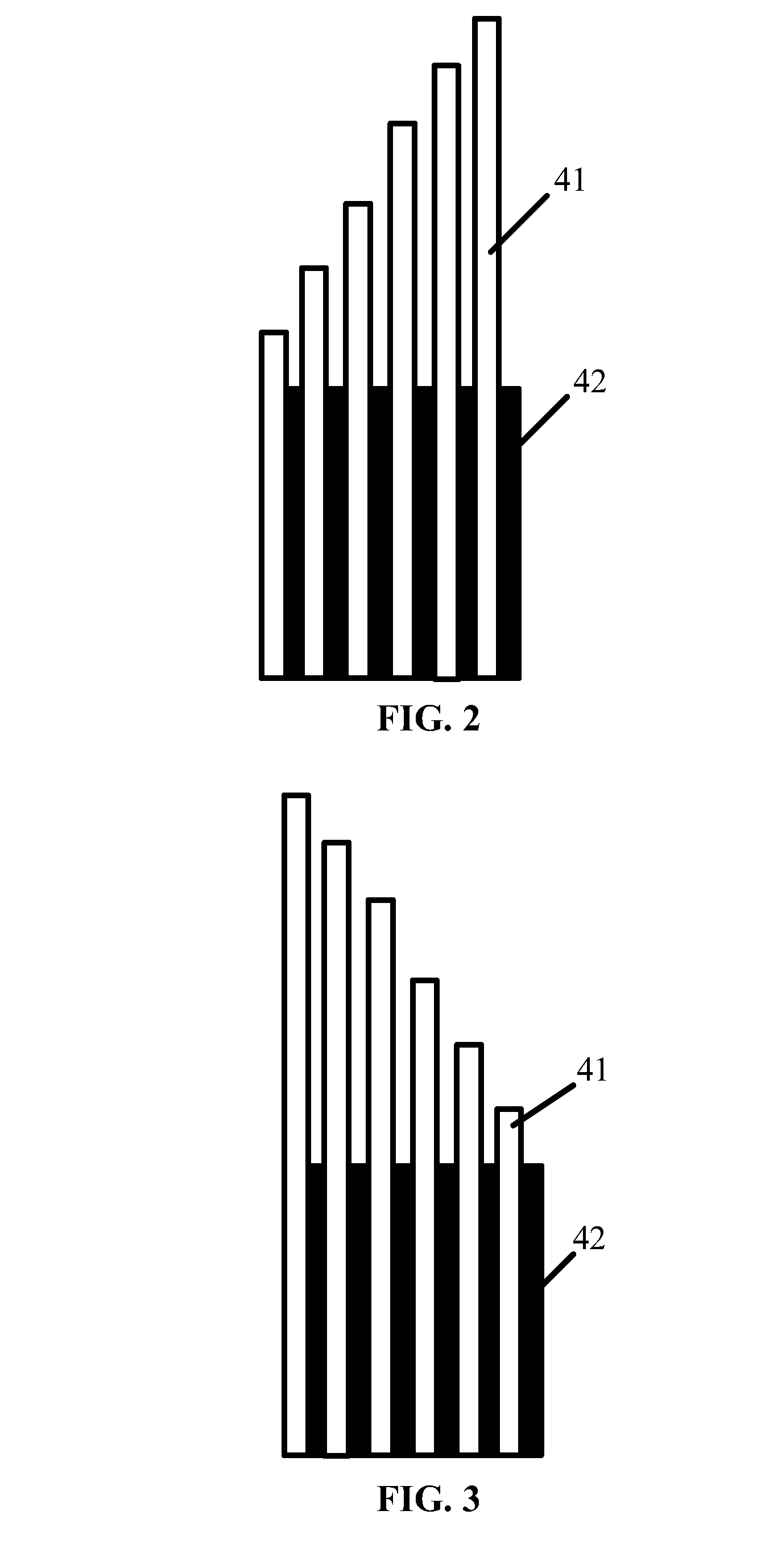
[0050]The semiconductor LED in Example 2 has the same structure as the abovementioned example. In this example, the distribution of Al component of the first AlGaN layers and the second AlGaN layers of the electron blocking layer is shown in FIG. 3. In FIG. 3, white boxes represent the first AlGaN layers, black boxes represent the second AlGaN layers, and the height of the boxes indicates the size of the content of the layer of Al components. A left side of the figure denotes the side of the quantum well layer, and a right side of the figure denotes the side of the p-GaN layer.

[0051]As shown in FIG. 3, in this example, from the side of the quantum well layer to the side of the p-GaN layer, namely from the left side to the right side, the Al component of the plurality of first AlGaN layers 41 is gradually decreased layer by layer, and the Al component of the plurality of second AlGaN layers 42 are invariable.

[0052]In this example, the electron blocking layer 40 may comprise, but not ...

example 3

[0057]The semiconductor LED in Example 3 has the same structure as the abovementioned example. In this example, the distribution of Al component of the first AlGaN layers and the second AlGaN layers of the electron blocking layer is shown in FIG. 4. In FIG. 4, white boxes represent the first AlGaN layers, black boxes represent the second AlGaN layers, and the height of the boxes indicates the size of the content of the layer of Al components. A left side of the figure denotes the side of the quantum well layer, and a right side of the figure denotes the side of the p-GaN layer.

[0058]As shown in FIG. 4, in this example, the Al component of the plurality of second AlGaN layers are invariable, the first AlGaN layer with lowest Al component is located in the middle portion of the electron blocking layer, from the first AlGaN layer with lowest Al component to the side of the quantum well layer, namely from middle portion to the left side, the Al component of the first AlGaN layers 41 is ...


PUM


Abstract

A semiconductor light-emitting diode, including: an n-GaN layer, a quantum well layer, an electron blocking layer, and a p-GaN layer, which are sequentially stacked on a substrate. The electron blocking layer includes at least one first AlGaN layer and at least one second AlGaN layer. The first AlGaN layer and the second AlGaN layer are alternately stacked. The adjacent first and second AlGaN layers have different Al component.

Description

CROSS-REFERENCE TO RELATED APPLICATIONS[0001]This application is a continuation-in-part of International Patent Application No. PCT / CN2012 / 079285 with an international filing date of Jul. 27, 2012, designating the United States, now pending, and further claims priority benefits to Chinese Patent Application No. 201210056382.0 filed Mar. 6, 2012. The contents of all of the aforementioned applications, including any intervening amendments thereto, are incorporated herein by reference. Inquiries from the public to applicants or assignees concerning this document or the related applications should be directed to: Matthias Scholl P. C., Attn.: Dr. Matthias Scholl Esq., 245 First Street, 18th Floor, Cambridge, Mass. 02142.BACKGROUND OF THE INVENTION[0002]1. Field of the Invention[0003]The present invention relates to a semiconductor light-emitting diode (LED) and method for manufacturing the same.[0004]2. Description of the Related Art[0005]The leakage of electrons is a main factor affect...

Claims


Application Information

Patent Timeline
Patent Type & Authority Applications(United States)
IPC IPC(8): H01L33/00H01L33/14H01L33/32H01L33/06
CPCH01L33/0025H01L33/06H01L33/32H01L33/145H01L33/0075H01L33/04
Inventor LI, WENBINGWANG, JIANGBODONG, BINZHONGYANG, CHUNYAN
Owner HC SEMITEK CORP
Why Eureka
Try Eureka