LED (Light Emitting Diode) and manufacturing method thereof

A technology of light-emitting diodes and manufacturing methods, which is applied in the direction of electrical components, circuits, semiconductor devices, etc., can solve the problems that cannot meet the needs of devices well, and the concentration of hole carriers is low, so as to improve luminous efficiency and increase hole density. effect of concentration

Inactive Publication Date: 2011-05-18
ENRAYTEK OPTOELECTRONICS
View PDF4 Cites 14 Cited by
  • Summary
  • Abstract
  • Description
  • Claims
  • Application Information

AI Technical Summary

Problems solved by technology

[0004] However, prior art light-emitting diodes suffer from the following disadvantages: the background carrier (electron) concentration of the light-emitting diode is too high, and the p-type doping level is low, which in turn leads to a too low hole carrier concentration
However, due to the high ionization energy of Mg (about 250 meV), even after low-energy electron beam irradiation (LEEBI) or rapid thermal annealing (RTA) process, part of Mg can be activated, and the hole concentration can reach 10 18 / cm 3 , but still not well enough to meet the device needs

Method used


Image

  • LED (Light Emitting Diode) and manufacturing method thereof
  • LED (Light Emitting Diode) and manufacturing method thereof
  • LED (Light Emitting Diode) and manufacturing method thereof

Examples


Embodiment Construction

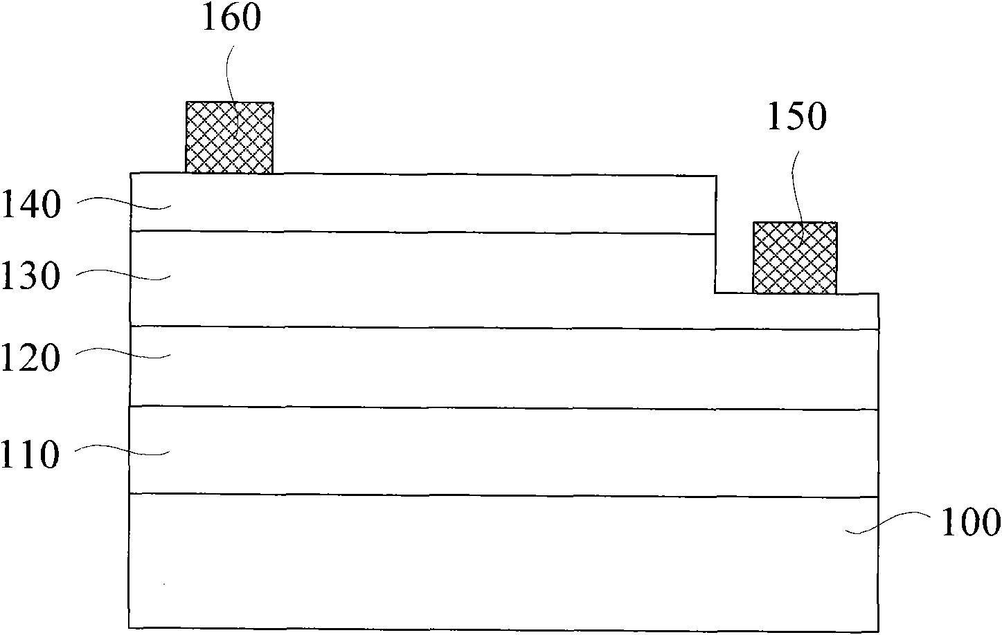
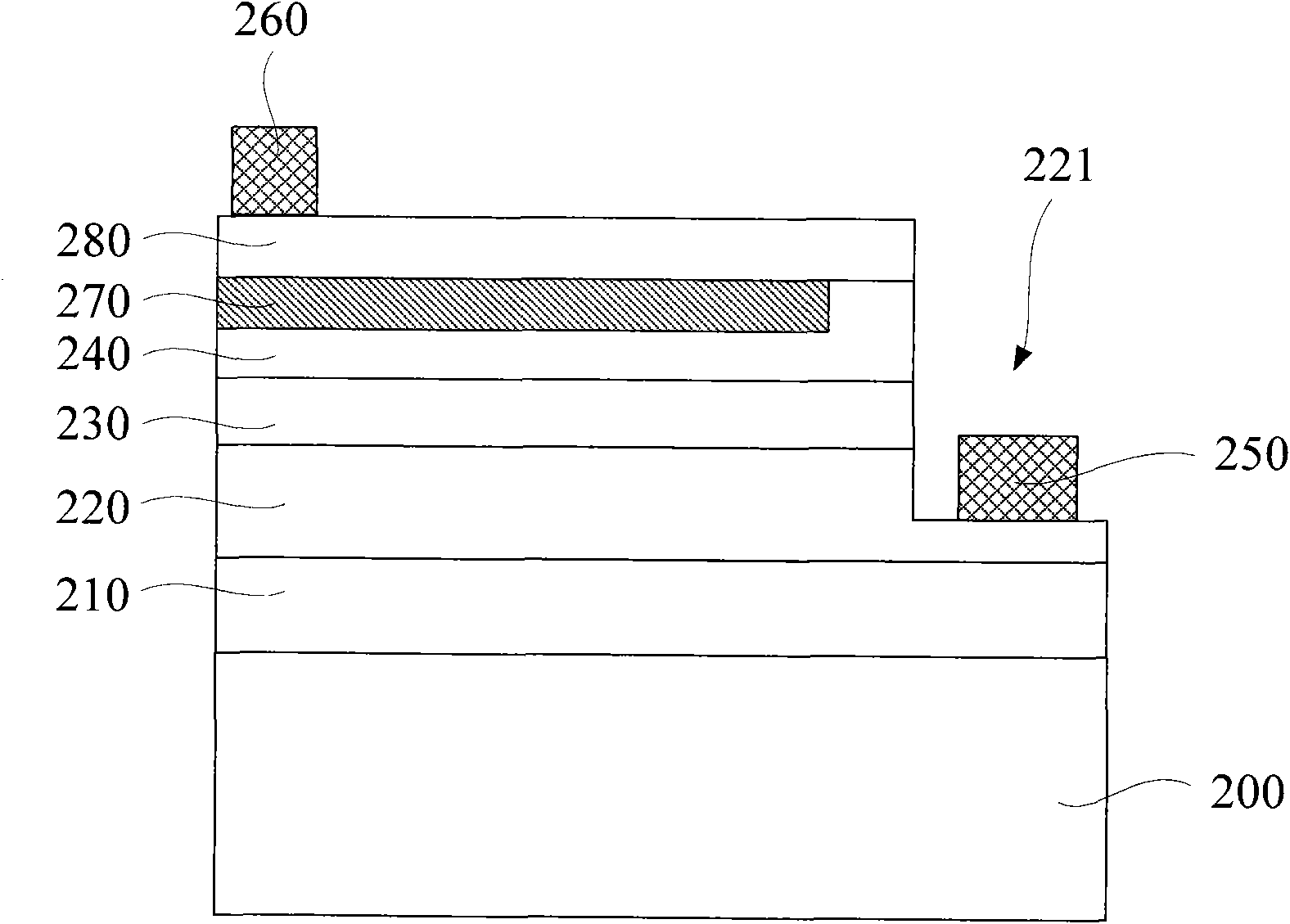
[0023] It has been mentioned in the background technology that the main obstacle to the development of the existing light-emitting diodes is that the background carrier (electron) concentration of the light-emitting diode is too high, and the p-type doping level is low, which in turn leads to the hole carrier concentration too low. Therefore, the present invention provides a light-emitting diode and a manufacturing method thereof. In the light-emitting diode, a p-type buried electrode layer is additionally formed in the p-type semiconductor layer. When the light-emitting diode emits light, the p-type buried electrode layer can enhance Concentration of holes that contribute to luminescence, thereby improving the luminous efficiency of light-emitting diodes.

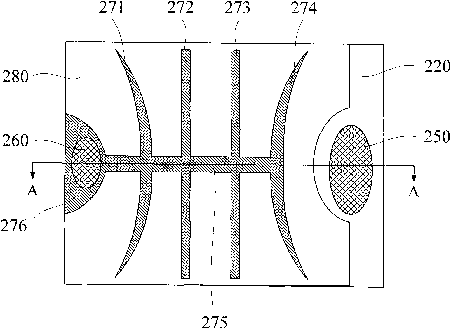
[0024] Please refer to figure 2 with image 3 ,in, figure 2 is a top view of the light emitting diode provided by the embodiment of the present invention, image 3 yes figure 2 The schematic cross-sectional view of...


PUM


Abstract

The invention discloses an LED (Light Emitting Diode) and a manufacturing method thereof. The LED comprises a substrate, an n-type semiconductor layer, an active layer, a p-type semiconductor layer, a p-type buried electrode layer, an opening, a first electrode and a second electrode. The n-type semiconductor layer, the active layer and the p-type semiconductor layer are sequentially arranged on the substrate. The p-type buried electrode layer is formed in the p-type semiconductor layer. The opening extends into the n-type semiconductor layer in depth. The first electrode is formed in the opening, and the n-type semiconductor layer is electrically connected with the negative electrode of a power source by the first electrode. The second electrode is formed on the p-type semiconductor layer, and the p-type semiconductor layer is electrically connected with the positive electrode of the power source by the p-type buried electrode layer. The p-type buried electrode layer can increase the hole concentration contributing to light emission so as to improve the light emitting efficiency of the LED.

Description

technical field [0001] The invention relates to the field of semiconductor light emitting, in particular to a light emitting diode and a manufacturing method thereof. Background technique [0002] Light Emitting Diode (LED, Light Emitting Diode) is used in various fields due to its advantages of long life and low energy consumption, especially as its lighting performance index is greatly improved day by day, LED is often used as a light emitting device in the lighting field. Among them, the III-V group compounds represented by gallium nitride (GaN) have the characteristics of wide band gap, high luminous efficiency, high electron saturation drift speed, and stable chemical properties. The field of devices has great application potential and has attracted widespread attention. [0003] For details, please refer to figure 1 , which is a schematic cross-sectional view of a light emitting diode in the prior art. Such as figure 1 As shown, an existing light-emitting diode inc...

Claims


Application Information

Patent Timeline
Patent Type & Authority Applications(China)
IPC IPC(8): H01L33/02H01L33/00H01L33/12H01L33/42
Inventor 张汝京
Owner ENRAYTEK OPTOELECTRONICS
Why Eureka
Try Eureka