Thin layer SOILIGBT device

A device and thin-layer technology, applied in semiconductor devices, electrical components, circuits, etc., can solve problems such as increasing process costs, and achieve the effects of reducing process difficulty and cost, small parasitic effects, and low leakage current.

Inactive Publication Date: 2009-05-13
UNIV OF ELECTRONICS SCI & TECH OF CHINA
View PDF0 Cites 13 Cited by
  • Summary
  • Abstract
  • Description
  • Claims
  • Application Information

AI Technical Summary

Problems solved by technology

Although the device uses a 5μm SOI layer, the P-type body region 9 and the N - The PN junction formed by the drift region 16 still increases additional parasitic capacitance compared with the thin-layer SOI technology, and requires additional process steps such as deep groove etching, groove filling, and planarization, which increases the process cost

Method used


Image

  • Thin layer SOILIGBT device
  • Thin layer SOILIGBT device
  • Thin layer SOILIGBT device

Examples


Embodiment Construction

[0025] By adopting the thin-layer SOI LIGBT of the present invention, high-voltage, high-speed, and low-conduction-loss power devices with excellent performance can be obtained, which can meet the requirements of high-voltage, high-current, and low-conduction power devices for driving stages such as 150-250V PDP row driver ICs and 600V switching power supply ICs. pass loss requirements.

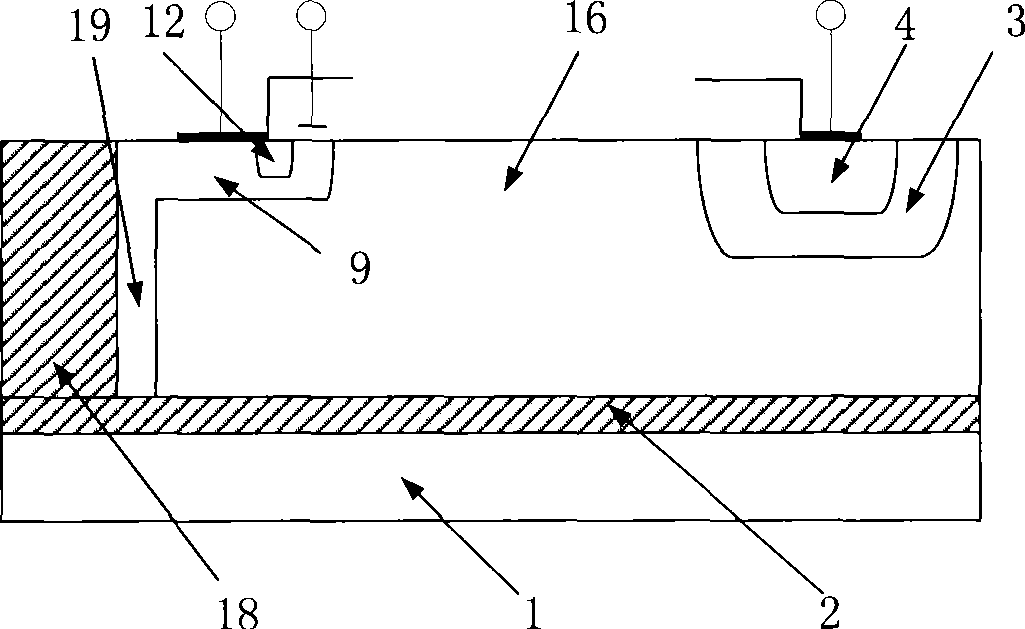
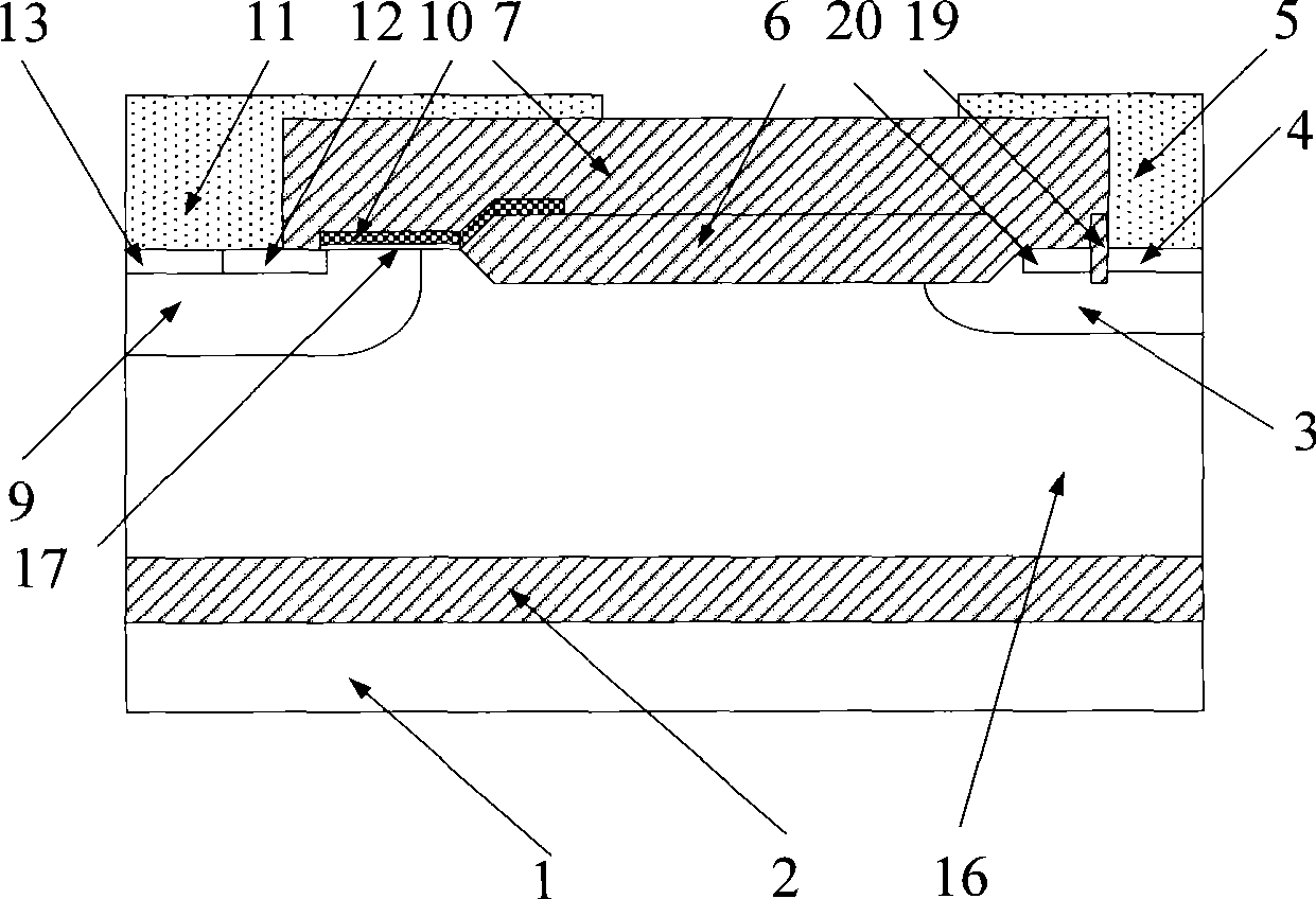
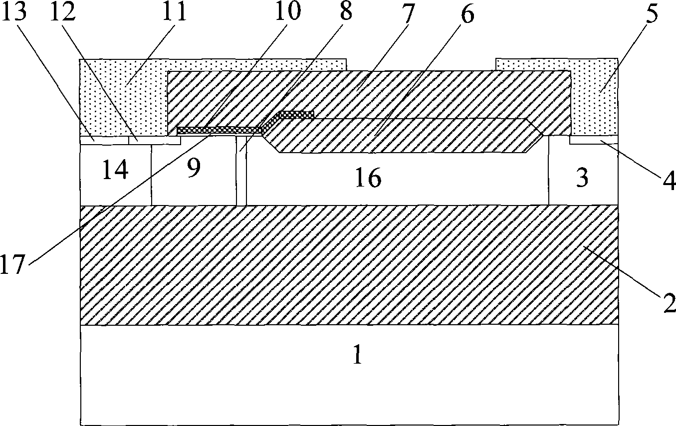
[0026] A kind of thin layer SOI LIGBT device provided by the present invention, such as image 3 As shown, including: substrate 1, buried oxide layer 2, N-type buffer layer 3, P + Anode region 4, anode metal 5, field oxygen region 6, pre-metal dielectric 7, N-type hole barrier layer 8, P-type body region 9, polysilicon gate 10, cathode metal 11, cathode N + Zone 12, Cathode P + Region 13, P-type region 14, N - Drift region 16 and gate oxide layer 17. The upper surface of the substrate 1 is a buried oxide layer 2, and the upper surface of the buried oxide layer 2 is an SOI layer with a thi...


PUM


Abstract

The invention relates to a folium SOILIGBT device which belongs to the technical field of semiconductor power device. The thickness of SOI layer of the device is 1 mu m to 2 mu m; a cavity barrier layer is arranged between a body zone and a drift zone; the cavity is blocked in the drift zone to the utmost extent; and then the cavity consistence near the side of a cathode in the drift zone is increased; and conduction losses of the device are reduced. A P type depletion zone can also be added near the cavity barrier layer to assist to deplete the N type cavity barrier layer, and so drift zone depletion is strengthened when the device bears a high pressure, and breakdown characteristics of the device are improved. The folium SOILIGBT device has the advantages of small parasitics, fast speed, low power consumption, strong anti-radiation performance, and is compatible with the standard process. An LIGBT device having good performance, high pressure, high speed and low conduction losses can be made when the folium SOILIGBT device is adopted.

Description

technical field [0001] The invention belongs to the technical field of semiconductor power devices. Background technique [0002] Lateral Insulated-Gate Bipolar Transistor LIGBT (Lateral Insulated-Gate Bipolar Transistor) is often used in the output stage of high-voltage power drive integrated circuits to improve the withstand voltage and The contradiction between the on-resistance. SOI technology has the advantages of ideal dielectric isolation performance, relatively simple dielectric isolation process, small parasitic effects, fast speed, low power consumption, high integration, and strong radiation resistance, making SOI LIGBT popular in the field of high-voltage power integrated circuits. received widespread attention. [0003] Literature (1) M.Stoisiek, K.-G.Oppermann, U.Schwalke, et al.A dielectric isolated high-voltage IC-technology for off-Line applications.1995 International Symposium on Power Semiconductor Devices and ICs, Vol.7: 325 -329, using SDB materials w...

Claims


Application Information

Patent Timeline
Patent Type & Authority Applications(China)
IPC IPC(8): H01L29/739H01L29/06
Inventor 乔明罗波廖红蒋苓利王卓张波
Owner UNIV OF ELECTRONICS SCI & TECH OF CHINA
Why Eureka
Try Eureka