AlGa-based semiconductor ultraviolet device for improving luminous efficiency and preparation method thereof

A semiconductor and ultraviolet technology, applied in the direction of semiconductor devices, electrical components, circuits, etc., can solve the problems of insufficient hole injection, electron leakage, unfavorable radiation recombination, etc., to reduce the height of the hole barrier, eliminate polarization charges, improve The effect of luminous efficiency

Pending Publication Date: 2018-06-29
GUANGDONG INST OF SEMICON IND TECH
View PDF8 Cites 12 Cited by
  • Summary
  • Abstract
  • Description
  • Claims
  • Application Information

AI Technical Summary

Problems solved by technology

However, the structure obtained in this way will move the valence band up and form a potential barrier to the holes, making the hole injection more insufficient and thus unfavorable for radiative recombination. At the same time, the insufficient hole injection will induce greater electron leakage.

Method used


Image

  • AlGa-based semiconductor ultraviolet device for improving luminous efficiency and preparation method thereof
  • AlGa-based semiconductor ultraviolet device for improving luminous efficiency and preparation method thereof
  • AlGa-based semiconductor ultraviolet device for improving luminous efficiency and preparation method thereof

Examples


Embodiment 1

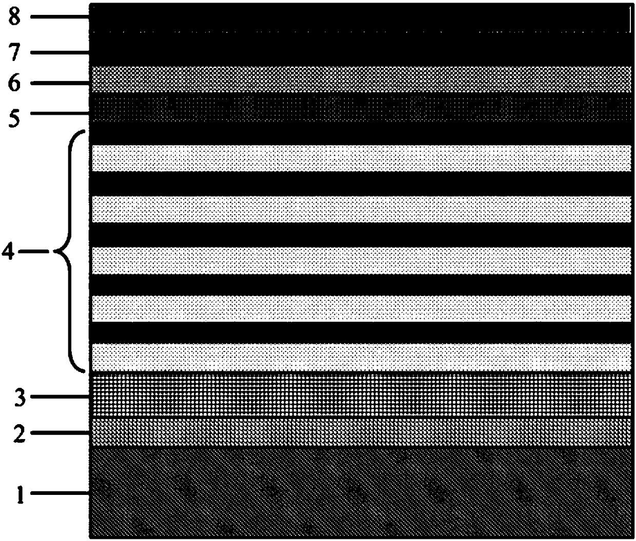
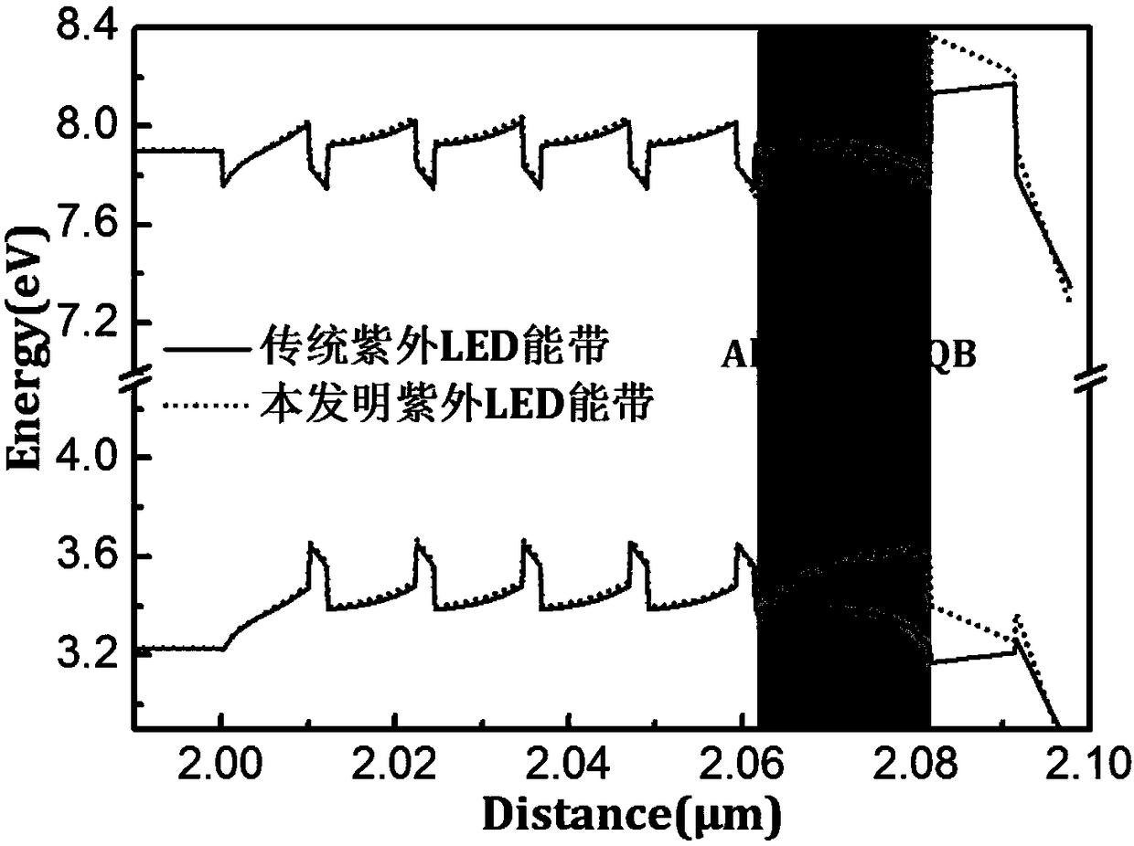
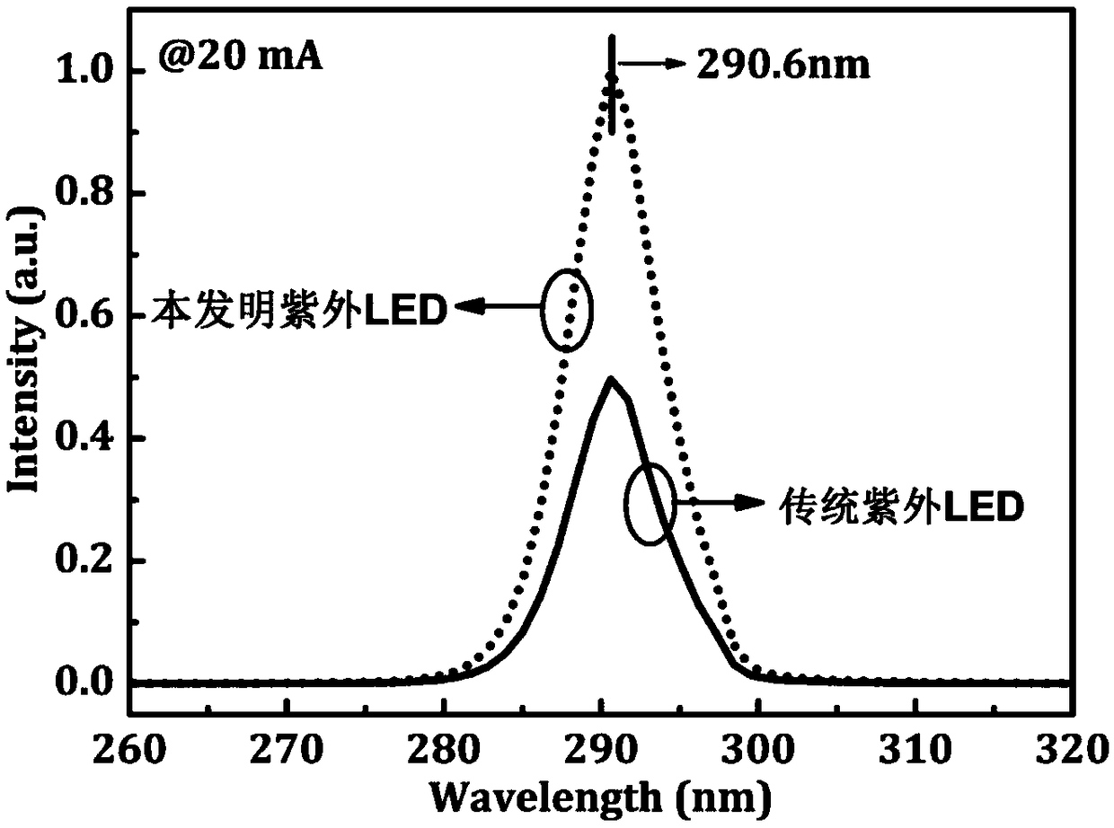
[0047] figure 1 A schematic structural diagram of an AlGaN-based semiconductor ultraviolet device with improved light efficiency provided by an embodiment of the present invention. figure 2 It is a comparison diagram of the energy bands of the traditional structure and the AlGaN-based ultraviolet LED of the present invention; image 3 It is a comparison chart of the electroluminescence spectra of the traditional structure and the AlGaN-based ultraviolet LED of the present invention. see Figure 1 to Figure 3 This embodiment provides an AlGaN-based semiconductor ultraviolet device with improved light efficiency. The epitaxial structure of the AlGaN-based semiconductor ultraviolet device with improved light efficiency includes a substrate 1, an AlN buffer layer 2, an n-type AlGaN layer 3, Al x Ga 1-x N / Al y Ga 1-y N light emitting active region 4, last AlGaN quantum barrier layer 5, p-type AlGaN electron blocking layer 6, p-type AlGaN layer 7 and contact layer 8, where 0....

Embodiment 2

[0064] Image 6 The third design of the last AlGaN quantum barrier layer structure provided for this embodiment. see Image 6 , this embodiment provides an AlGaN-based semiconductor ultraviolet device with improved light efficiency. The difference between the AlGaN-based semiconductor ultraviolet device with improved light efficiency and the AlGaN-based semiconductor ultraviolet device with improved light efficiency provided in Embodiment 1 is that the ultraviolet device has The last AlGaN quantum barrier layer 5 set by the epitaxial structure, in Al x Ga 1-x N / Al y Ga 1-y On the N light-emitting active region 4; the specific changes are as follows: the aluminum component in the last AlGaN quantum barrier layer 5 first gradually decreases and then gradually rises along the growth direction, and the aluminum components in this thin layer respectively contact the last The quantum well and the p-type AlGaN electron blocking layer are the highest, and the aluminum composition...

Embodiment 3

[0067] Figure 8 The fifth design of the last AlGaN quantum barrier layer structure provided in this embodiment. see Figure 8 , this embodiment provides an AlGaN-based semiconductor ultraviolet device with improved light efficiency. The difference between the AlGaN-based semiconductor ultraviolet device with improved light efficiency and the AlGaN-based semiconductor ultraviolet device with improved light efficiency provided in Embodiment 1 is that the ultraviolet device has The last AlGaN quantum barrier layer 5 set by the epitaxial structure is in Al x Ga 1-x N / Al y Ga 1-y On the N light-emitting active region 4; the specific changes are as follows: the last AlGaN quantum barrier layer structure is composed of two groups of thin layers of Al-GaN layers with decreasing aluminum composition, and the aluminum composition between the two groups is Different; the closer to the P region, the lower the aluminum content of the thin layer of AlGaN layer, until the lowest alumin...


PUM


Abstract

The present invention provides an AlGa-based semiconductor ultraviolet device for improving luminous efficiency and a preparation method thereof, and relates to the technical field of semiconductors.The epitaxial structure of the device comprises a substrate, an AlN buffer layer, an n-type AlGaN layer, an AlxGa1-xN/AlyGa1-yN luminescence active region, the last one AlGaN quantum barrier layer, ap-type AlGaN electron blocking layer, a p-type AlGaN layer and a contact layer, wherein 0.01<=x and y<=1. The luminescence active region comprises a plurality of quantum well layers and a plurality ofquantum barrier layers, the quantum well layers and the quantum barrier layers are alternately arranged, and the last one AlGaN quantum barrier layer is an aluminium ingredient gradient layer. The last one AlGaN quantum barrier layer of aluminium ingredient gradient is introduced in the ultraviolet device to optimize the energy band structure of the device, effectively improve the electron restriction effect and enhance the cavity injection efficiency so as to improve the quantum efficiency and the luminescence efficiency of the semiconductor ultraviolet device.

Description

technical field [0001] The invention relates to the technical field of semiconductors, and in particular to an AlGaN-based semiconductor ultraviolet device with improved light efficiency and a preparation method thereof. Background technique [0002] In recent years, it has experienced exceptionally rapid development. According to reports, the theoretical maximum efficiency of white LEDs is as high as 400lm / W, far exceeding traditional lighting fixtures (incandescent lamps, fluorescent lamps, etc.). Although GaN-based LEDs have achieved good development, there is still a lot of room for development compared to their theoretical maximum efficiency. A key factor limiting the luminous efficiency of GaN-based LEDs is the electron current leakage caused by the mismatch of electron hole injection under high current conditions. Part of the electrons cannot fully recombine in the light-emitting active region, but leak from the active region to the p-type Area. [0003] With the d...

Claims


Application Information

Patent Timeline
Patent Type & Authority Applications(China)
IPC IPC(8): H01L33/00H01L33/06H01L33/32
CPCH01L33/0075H01L33/06H01L33/325
Inventor 贺龙飞陈志涛赵维张康吴华龙何晨光
Owner GUANGDONG INST OF SEMICON IND TECH
Why Eureka
Try Eureka