Semiconductor device

Inactive Publication Date: 2015-01-01
SEMICON ENERGY LAB CO LTD
View PDF9 Cites 29 Cited by
  • Summary
  • Abstract
  • Description
  • Claims
  • Application Information

AI Technical Summary

Benefits of technology

[0020]In accordance with one embodiment of the present inven

Problems solved by technology

Although a transistor including an oxide semiconductor can obtain transistor characteristics relatively easily, ph

Method used


Image

  • Semiconductor device
  • Semiconductor device
  • Semiconductor device

Examples


embodiment 1

[0048]In this embodiment, an oxide semiconductor layer included in a semiconductor device of one embodiment of the present invention will be described with reference to FIGS. 1A and 1B, FIGS. 2A and 2B, FIGS. 3A and 3B, FIGS. 4A to 4E, FIG. 5, FIGS. 6A to 6D, FIG. 7, FIGS. 8A to 8F, FIG. 9, FIGS. 10A and 10B, and FIG. 11.

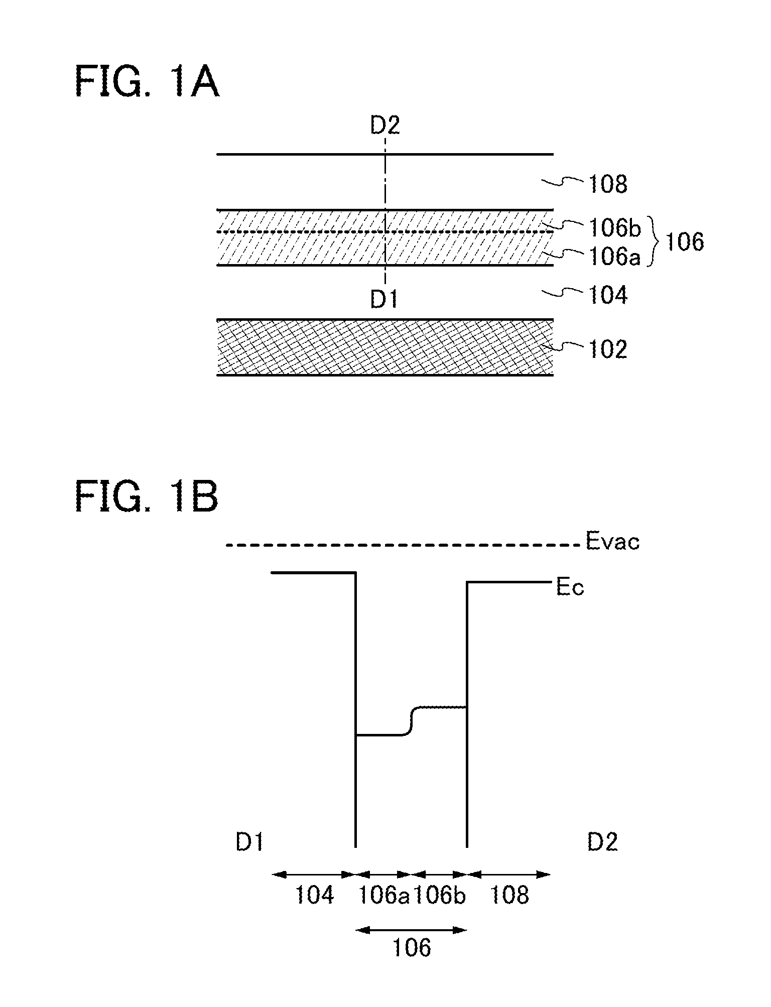
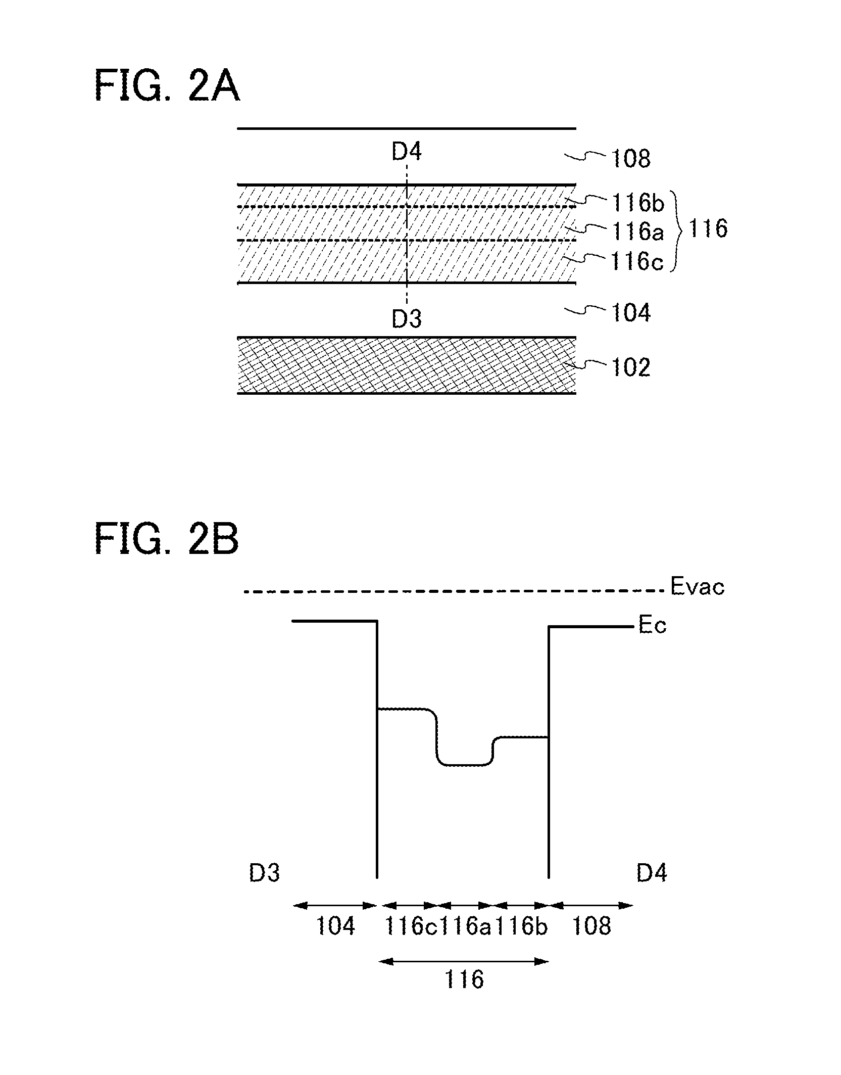
[0049]FIG. 1A is a schematic view exemplifying a stacked-layer structure included in a semiconductor device of one embodiment of the present invention. The semiconductor device of one embodiment of the present invention has a stacked-layer structure of a gate electrode layer 102, a gate insulating layer 104 over the gate electrode layer 102, an oxide semiconductor layer 106 over the gate insulating layer 104, and an insulating layer 108 over the oxide semiconductor layer 106.

[0050]The oxide semiconductor layer 106 has a stacked-layer structure of a first layer 106a and a second layer 106b which is between the first layer 106a and the insulating layer 108.

[0051]The f...

embodiment 2

[0126]In this embodiment, a semiconductor device having the stacked-layer structure described in Embodiment 1 is described with reference to FIGS. 12A to 12C, FIGS. 13A to 13C, FIGS. 14A to 14E, FIGS. 15A to 15C, FIGS. 16A to 16C, and FIGS. 17A to 17D.

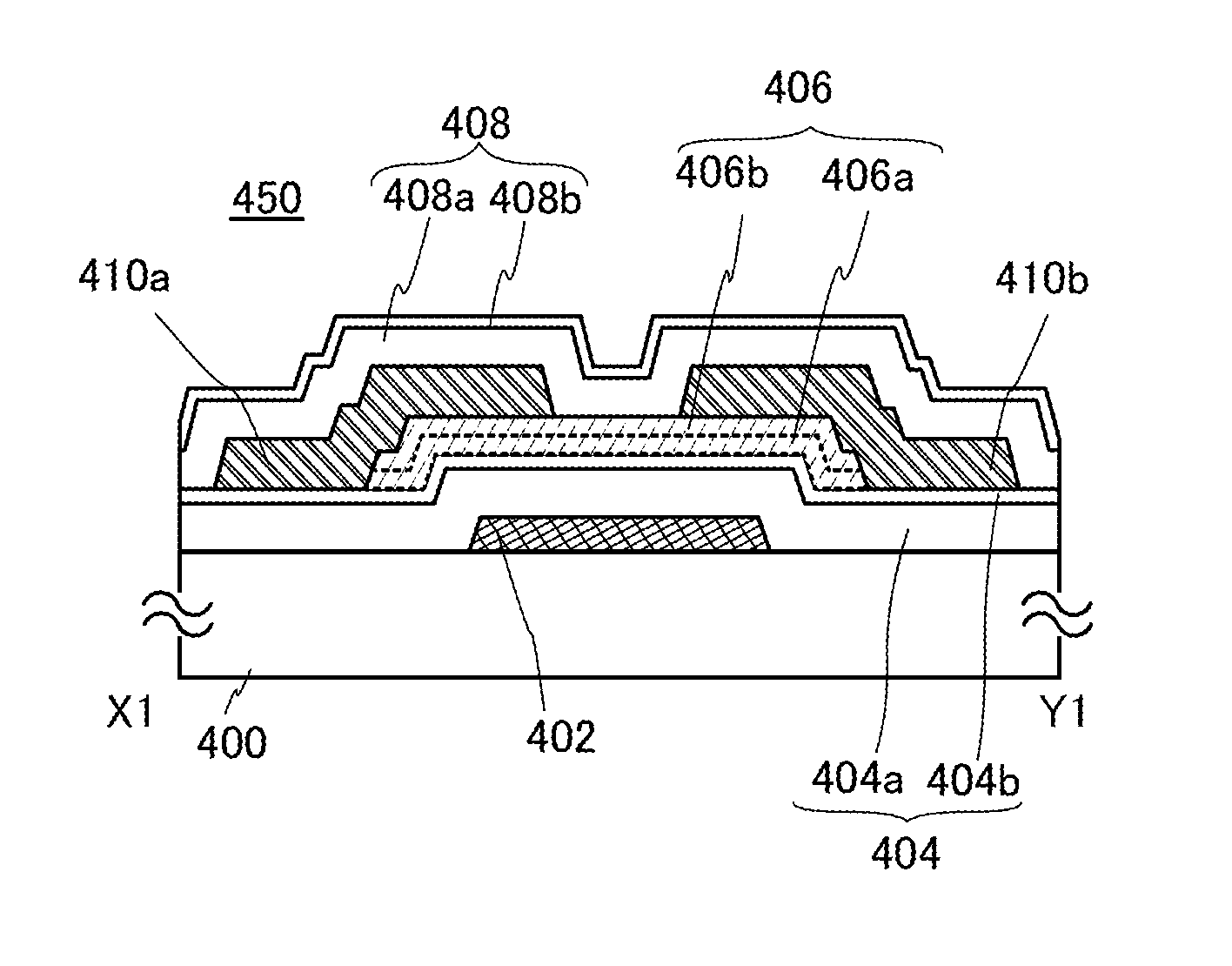
[0127]FIGS. 12A to 12C illustrate a structure example of a semiconductor device. FIGS. 12A to 12C illustrate a bottom-gate transistor as an example of a semiconductor device. FIG. 12A is a plan view of a transistor 450, FIG. 12B is a cross-sectional view taken along line V1-W1 in FIG. 12A, and FIG. 12C is a cross-sectional view taken along line X1-Y1 in FIG. 12A. Note that in FIG. 12A, some components of the transistor 450 (e.g., an insulating layer 408) are not illustrated for clarity. The same applies to other plan views.

[0128]The transistor 450 illustrated in FIGS. 12A to 12C includes a gate electrode layer 402 provided over a substrate 400, a gate insulating layer 404 over the gate electrode layer 402, an oxide semiconductor layer ...

embodiment 3

[0222]FIG. 18A illustrates an example of a circuit diagram of a NOR circuit, which is a logic circuit, as an example of the semiconductor device of one embodiment of the present invention. FIG. 18B is a circuit diagram of a NAND circuit.

[0223]In the NOR circuit in FIG. 18A, p-channel transistors 801 and 802 are transistors in each of which a channel formation region is formed using a semiconductor material (e.g., silicon) other than an oxide semiconductor, and n-channel transistors 803 and 804 each include an oxide semiconductor and each have a structure similar to any of the structures of the transistors described in Embodiment 2.

[0224]A transistor including a semiconductor material such as silicon can easily operate at high speed. In contrast, a charge can be held in a transistor including an oxide semiconductor for a long time owing to its characteristics.

[0225]To miniaturize the logic circuit, it is preferable that the n-channel transistors 803 and 804 be stacked over the p-chan...


PUM


Abstract

To provide a highly reliable semiconductor device including an oxide semiconductor. The device has a stacked-layer structure including an oxide semiconductor layer and an insulating layer in contact therewith. The oxide semiconductor layer includes a first layer where a channel is formed and a second layer which is between the first layer and the insulating layer and whose energy of the bottom of the conduction band is closer to the vacuum level than that of the first layer. The second layer serves as a barrier layer preventing formation of defect states between the channel and the insulating layer. The first layer and the second layer include a minute crystal part in which periodic atomic arrangement is not observed macroscopically or long-range order in atomic arrangement is not observed macroscopically. For example, a region with a size of 1 nm to 10 nm includes a crystal part having periodic atomic order.

Description

BACKGROUND OF THE INVENTION[0001]1. Field of the Invention[0002]The invention disclosed in this specification relates to a semiconductor device and a method for manufacturing the semiconductor device.[0003]In this specification and the like, a “semiconductor device” generally refers to a device which can function by utilizing semiconductor characteristics: an electro-optical device, a semiconductor circuit, a display device, a light-emitting device, and an electronic device are all included in the category of the semiconductor device.[0004]2. Description of the Related Art[0005]A technique by which a transistor is formed using a semiconductor film formed over a substrate having an insulating surface has attracted attention. The transistor is applied to a wide range of electronic devices such as an integrated circuit (IC) and an image display device (also simply referred to as a display device). As a semiconductor film applicable to the transistor, a silicon-based semiconductor mater...

Claims


Application Information

Patent Timeline
IPC IPC(8): H01L29/786
CPCH01L29/7869H01L29/78696H01L29/78606H01L29/0657H01L27/1225H01L29/04H01L29/42384H01L27/127
Inventor KUWABARA, HIDEAKIENDO, YUTATATEISHI, MARITAKAHASHI, MASAHIRO
Owner SEMICON ENERGY LAB CO LTD
Why Eureka
Try Eureka