Image element, and imaging device and imaging method using the same

Active Publication Date: 2015-01-08
FUJIFILM CORP
View PDF6 Cites 22 Cited by
  • Summary
  • Abstract
  • Description
  • Claims
  • Application Information

AI Technical Summary

Benefits of technology

[0017]According to any one of the aspects, an imaging element which may achieve satisfactory imaging quality rega

Problems solved by technology

However, when the zoom magnification is high, the pixel cell at the periphery does not sufficiently receive the light so that the uneven sensitivity may be caused.
As described above, even tho

Method used


Image

  • Image element, and imaging device and imaging method using the same
  • Image element, and imaging device and imaging method using the same
  • Image element, and imaging device and imaging method using the same

Examples


Example

[0031]Hereinafter, an embodiment of the present invention will be described with reference to the drawings.

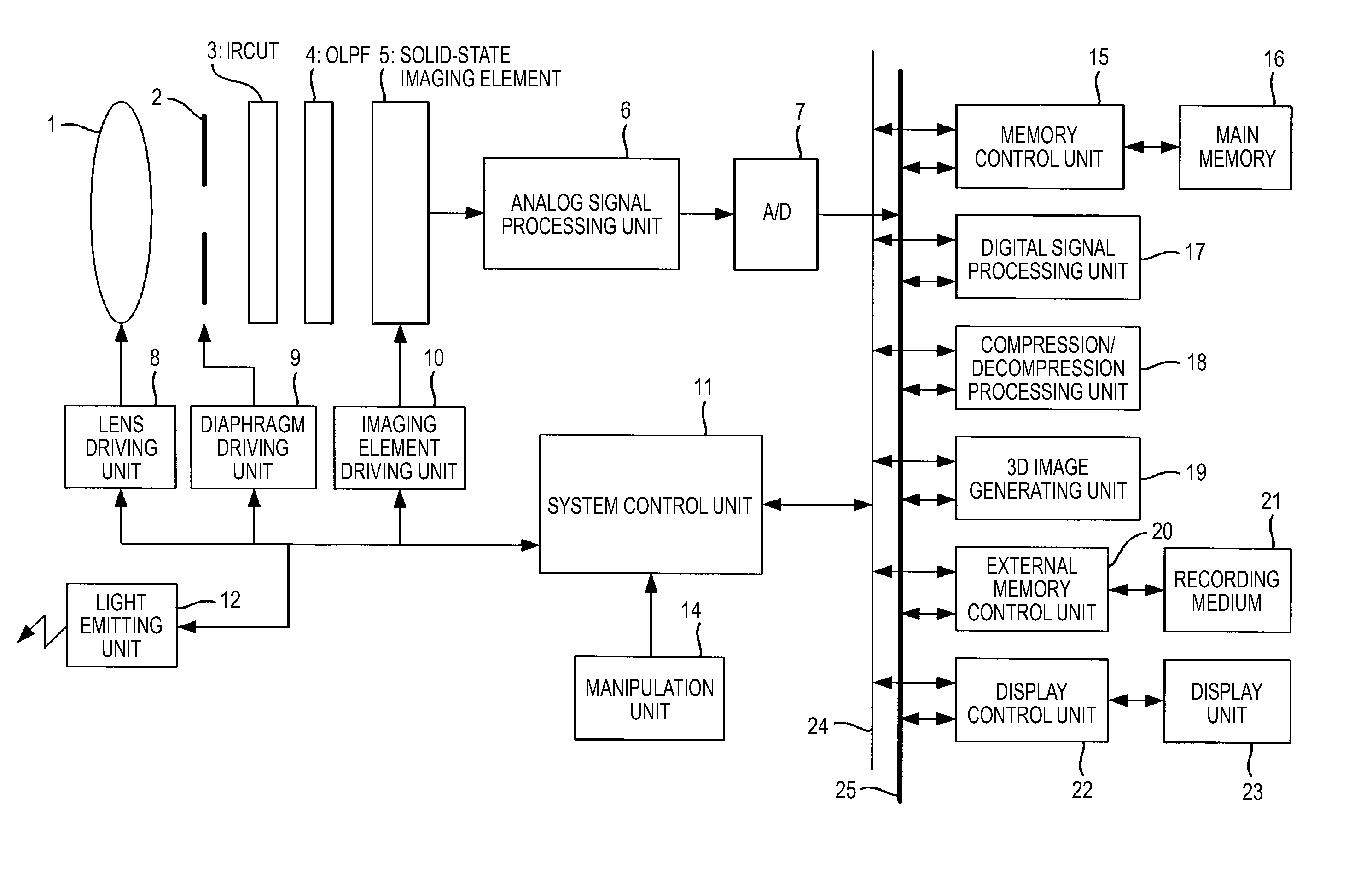
[0032]FIG. 1 is a diagram illustrating a schematic configuration of a digital camera which is an example of an imaging device for explaining an embodiment of the present invention.

[0033]An imaging system of an illustrated digital camera includes a single photographing optical system 1 which includes a focus lens and a zoom lens, a solid-state imaging element 5 such as a CCD image sensor or a CMOS image sensor, a diaphragm 2 which is provided between the photographing optical system 1 and the solid-state imaging element 5, an infrared cut filter 3, and an optical low-pass filter 4.

[0034]A system control unit 11 which integrally and collectively controls an entire electrical control system of the digital camera controls a flash light emitting unit 12. Further, the system control unit 11 controls a lens driving unit 8 to adjust a position of a focus lens which is included in the p...


PUM


Abstract

An imaging element which outputs a pair of image signals corresponding to a pair of luminous fluxes which pass through different pupil areas of a photographing optical system, the imaging element includes a first pixel cell group including a plurality of first pixel cells for obtaining the pair of image signals and a second pixel cell group including a plurality of second pixel cells for obtaining the pair of image signals. The first pixel cell includes a first photoelectric converting unit and a first micro lens which is provided above the first photoelectric converting unit. The second pixel cell includes a second photoelectric converting unit and a second micro lens which is provided above the second photoelectric converting unit. The first micro lens and the second micro lens are disposed with different regularities.

Description

CROSS REFERENCE TO RELATED APPLICATION[0001]This is a continuation of International Application No. PCT / JP2013 / 053033 filed on Feb. 8, 2013, and claims priority from Japanese Patent Application No. 2012-074307 filed on Mar. 28, 2012, the entire disclosures of which are incorporated herein by reference.BACKGROUND[0002]1. Technical Field[0003]The present invention relates to an imaging element, and an imaging device and an imaging method using the same.[0004]2. Related Art[0005]Recently, as the resolution of a solid-state imaging element such as a charge coupled device (CCD) image sensor and a complementary metal oxide semiconductor (CMOS) image sensor becomes higher, a demand for an information device having an imaging function such as a digital still camera, a digital video camera, a cellular phone such as a smart phone, and a personal digital assistant (PDA) is rapidly increasing. In the meantime, the information device having an imaging function as described above is referred to a...

Claims


Application Information

Patent Timeline
IPC IPC(8): H04N5/232H04N5/341H04N9/04
CPCH04N5/23212H04N5/341H04N9/045H04N5/23296G02B7/34H01L27/14621H01L27/14627H04N23/661H04N23/672H04N23/667H04N23/63H04N23/69H04N25/40H04N25/702H04N25/704H04N25/134
Inventor KOBAYASHI
Owner FUJIFILM CORP
Why Eureka
Try Eureka