Imaging apparatus having electron source array that emits electrons during a blanking period

a technology of electron source array and electron source, which is applied in the field of imaging apparatus, can solve the problems of not being able to read out all, affecting the image quality of the image, and generating large amount of holes in the image, so as to prevent the generation of capacitive or photoconductive residual images, improve image quality, and prevent the effect of image resolution degradation

Inactive Publication Date: 2010-11-16
FUTABA CORPORATION +1
View PDF4 Cites 8 Cited by
  • Summary
  • Abstract
  • Description
  • Claims
  • Application Information

AI Technical Summary

Benefits of technology

[0032]According to at least one embodiment, the imaging apparatus can prevent the degradation of image resolution resulting from blooming occurring due to highly bright incident light, and can also prevent the generation of capacitive or photoconductive residual images. Satisfactory image quality is thus obtained.

Problems solved by technology

Consequently, the output video image suffers an artifact by which a highly bright object appears expanded from its original size (which will hereinafter be referred to as “blooming”), degrading image quality such as image resolution.
Further, when highly bright light enters a portion of the photoelectric conversion film, a large amount of holes are generated and accumulated in this portion.
When this happens, it may not be possible to read out all the generated and accumulated holes by use of the electrons emitted from the electron emission array on a single scan, thereby creating a prominent capacitive residual image.
Moreover, the entry of highly bright light into the photoelectric conversion film causes a large amount of holes to be accumulated on the electron scan side of the photoelectric conversion film.
This serves to drop the effective electric field applied to the photoelectric conversion film, resulting in a large amount of optically generated electric charge (electrons and holes) being trapped in the photoelectric conversion film.
In the imaging device disclosed in Patent Document 2, however, the amount of electrons used to remove excessively accumulated electric charge is limited to the amount of electrons that are emitted during a single excessively-accumulated charge sweeping period within one field or one frame.
The effect of electric charge removal thus may not be sufficient depending on imaging conditions.
It is thus not possible to remove all the excessive holes generated and accumulated in the photoelectric conversion film within a single excessively-accumulated charge sweeping period.
In this case, image degradation is unavoidable due to the lowering of image resolution resulting from blooming and also due to the generation of capacitive residual images.
This gives rise to a problem that blooming is generated, and image resolution is degraded.
Further, the imaging device disclosed in Patent Document 2 cannot prevent the generation of a photoconductive residual image resulting from the lowering of an electric field within the photoelectric conversion film in response to highly bright incident light.
This causes a severe reduction in image quality.

Method used


Image

  • Imaging apparatus having electron source array that emits electrons during a blanking period
  • Imaging apparatus having electron source array that emits electrons during a blanking period
  • Imaging apparatus having electron source array that emits electrons during a blanking period

Examples


first embodiment

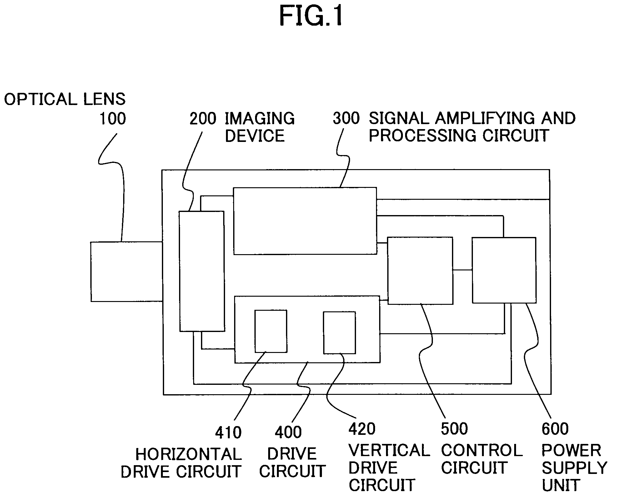
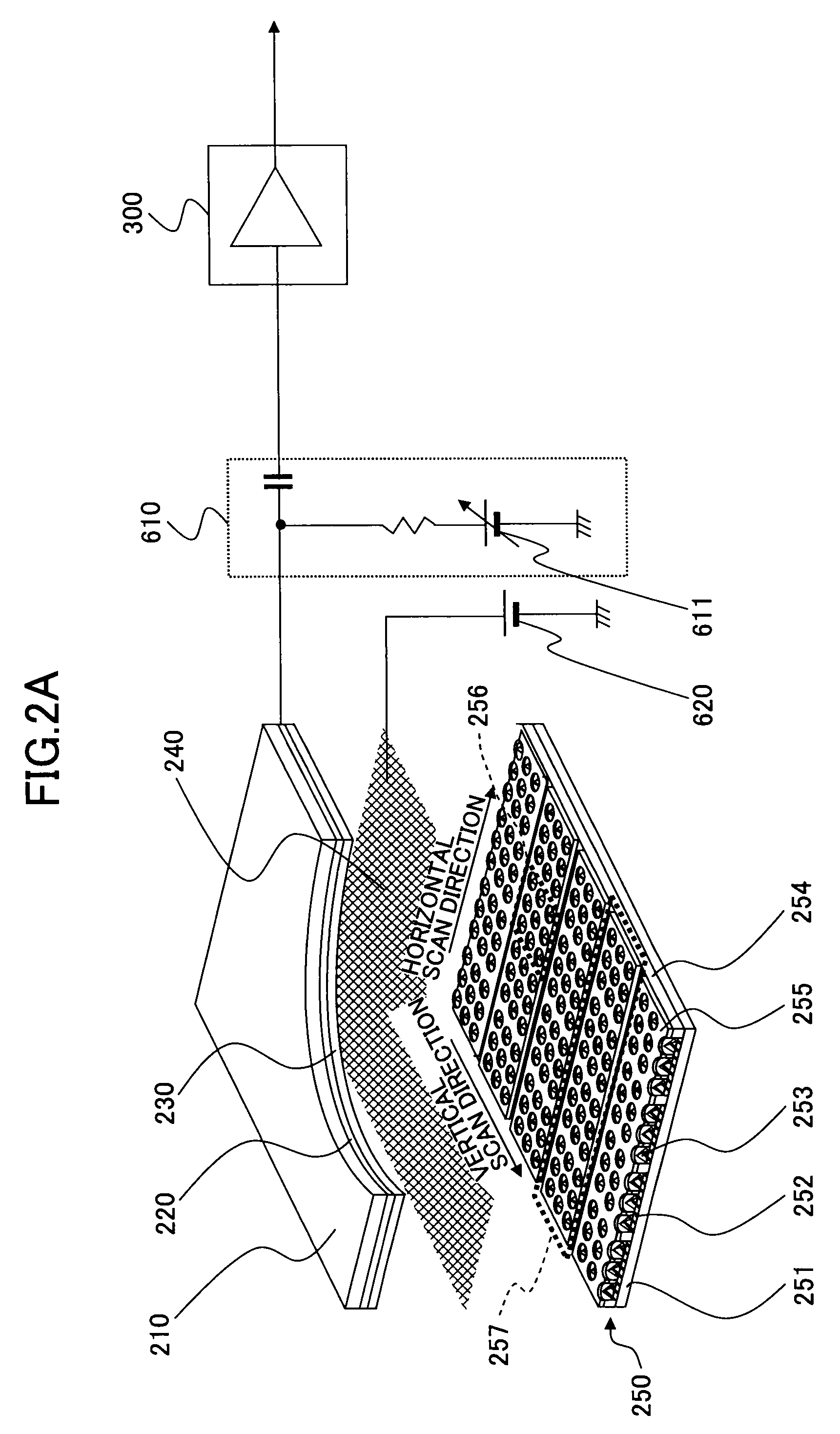
[0069]FIG. 1 is a schematic cross-sectional view of an imaging apparatus according to a first embodiment. The imaging apparatus of this embodiment includes an optical lens 100, an imaging device 200, a signal amplifying and processing circuit 300, a drive circuit 400, a control circuit 500, and a power supply unit 600.

[0070]The optical lens 100 and the imaging device 200 are arranged such that light passing through the optical lens 100 enters the photoelectric conversion film of the imaging device 200 perpendicularly to form a focus thereon.

[0071]The signal amplifying and processing circuit 300 amplifies and processes video signals output from the imaging device 200.

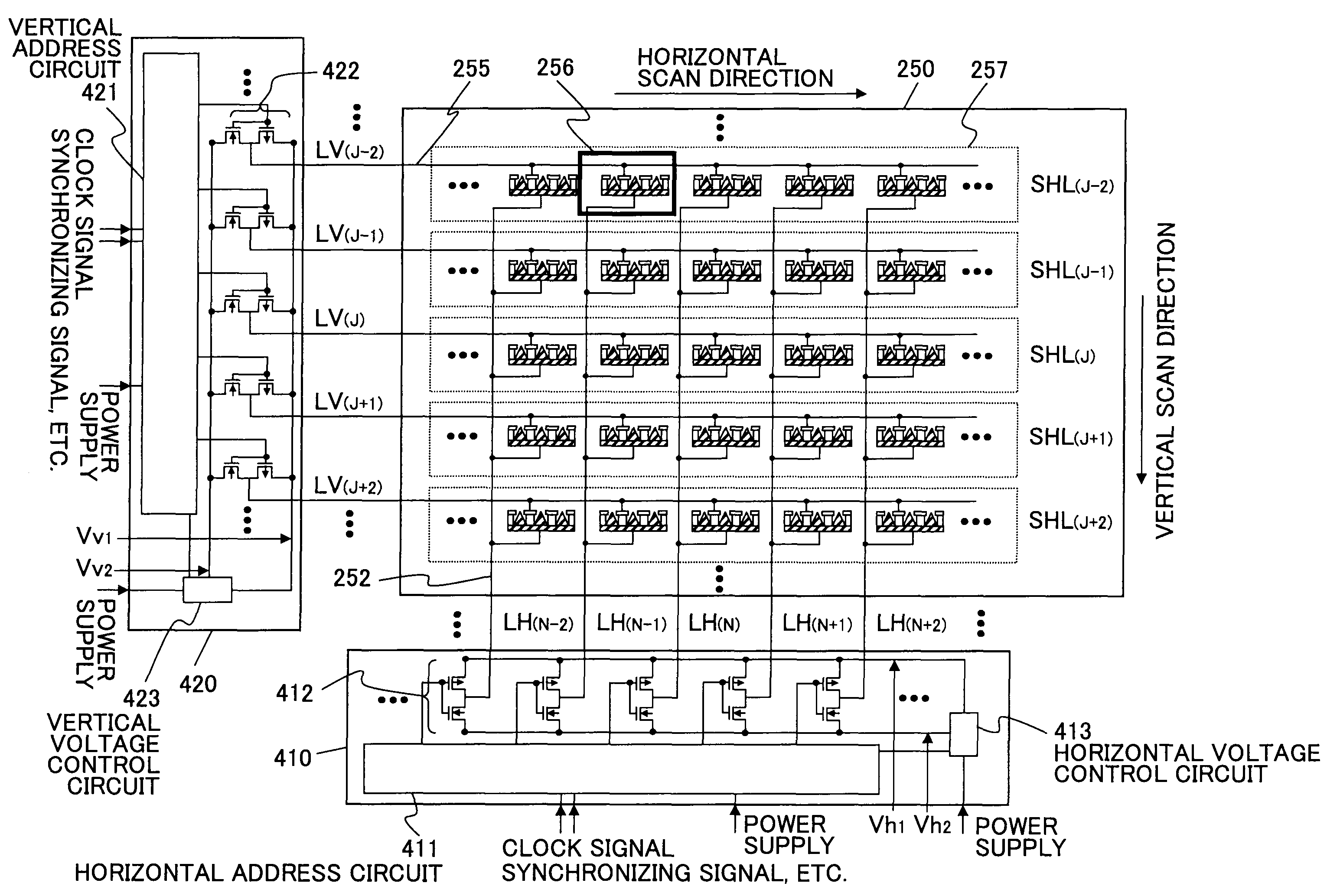
[0072]The drive circuit 400 includes a horizontal drive circuit 410, a vertical drive circuit 420, etc., and generates pulse voltages necessary to drive the imaging device 200.

[0073]The control circuit 500 generates a clock signal, synchronizing signals, and the like, and supplies these signals to the drive circuit 400 a...

second embodiment

[0155]FIG. 18 is a schematic cross-sectional view of an imaging apparatus according to a second embodiment. The imaging apparatus of the present embodiment differs from the imaging apparatus of the first embodiment in that a memory unit 700 is provided. Due to the provision of the memory unit 700, the configuration and operation of the imaging device 200 also differ from those of the first embodiment. In the following, a description will be given mainly with respect to such differences. The same elements as those of the imaging apparatus of the first embodiment are referred to by the same numerals, and a description thereof will be omitted.

[0156]The memory unit 700 serves to record and store video signals output from the signal amplifying and processing circuit 300. The memory unit 700 may be implemented by use of a known volatile or nonvolatile memory.

[0157]A control circuit 500A reads a video signal that is recorded and stored in the memory unit 700. The control circuit 500A gener...


PUM


Abstract

An imaging apparatus includes an electron emission array having electron sources arranged in matrix form and having a plurality of horizontal scan lines, a photoelectric conversion film opposed to the electron emission array, and a control and drive circuit configured to select one or more of the horizontal scan lines in a given video signal output period and to cause the electron sources included in the selected one or more horizontal scan lines to emit electrons toward the photoelectric conversion film to produce a video signal, wherein the control and drive circuit is configured to cause the electron sources included in unselected one or more horizontal scan lines not selected in the given video signal output period to emit electrons toward the photoelectric conversion film in a blanking period immediately preceding the given video signal output period.

Description

BACKGROUND OF THE INVENTION[0001]1. Field of the Invention[0002]The disclosures herein relate to an imaging apparatus provided with a photoelectric conversion film and an electron source array having electron sources arranged in matrix form wherein electrons are emitted from the electron source array during a video signal output period and a vertical blanking period.[0003]2. Description of the Related Art[0004]Research has been conducted for some time with respect to imaging apparatus that is provided with a photoelectric conversion film and an electron emission array having a matrix of electron emission sources, from which electrons are drawn out by an electric field without application of heat. This electron emission array has a plurality of Spindt-type emitters arranged in matrix form, which are opposed to the photoelectric conversion film across vacuum space. In such imaging device, holes that are generated and accumulated in the photoelectric conversion film in response to ligh...

Claims


Application Information

Patent Timeline
Patent Type & Authority Patents(United States)
IPC IPC(8): H01L31/00G09G3/20
CPCH01J31/38H01J31/49H04N5/217H04N5/30H04N23/81
Inventor NAMBA, MASAKAZUHONDA, YUKIHIRANO, YOSHIYUKIOKAZAKI, SABUROEGAMI, NORIFUMIWATABE, TOSHIHISATAKIGUCHI, YOSHIROKOBAYASHI, AKIRAITOH, SHIGEOTANIGUCHI, MASATERUNAKAMURA, KAZUHITOMIYA, KENTAOKUDA, YOSHIYUKINEGISHI, NOBUYASU
Owner FUTABA CORPORATION
Why Eureka
Try Eureka