Printed circuit board and manufacture method thereof

a technology of printed circuit boards and manufacturing methods, applied in the direction of printed circuits, printed circuit components, printed circuit non-printed electric components association, etc., can solve the problems of not meeting the recent trend toward slimness of electronic products, and the thickness of the entire printed circuit board becomes thick

Inactive Publication Date: 2015-01-22
SAMSUNG ELECTRO MECHANICS CO LTD
View PDF11 Cites 10 Cited by
  • Summary
  • Abstract
  • Description
  • Claims
  • Application Information

AI Technical Summary

Benefits of technology

[0011]An object of the present invention is to provide a printed circuit board capable of implementing slimness of the enti...

Problems solved by technology

However, in the printed circuit board manufactured as described above, as the insulating layer is uniformly laminated on both surfaces of the core layer embedd...

Method used


Image

  • Printed circuit board and manufacture method thereof
  • Printed circuit board and manufacture method thereof
  • Printed circuit board and manufacture method thereof

Examples


Embodiment Construction

[0028]Hereinafter, preferable embodiments of the present invention will be described in detail with reference to the accompanying drawings.

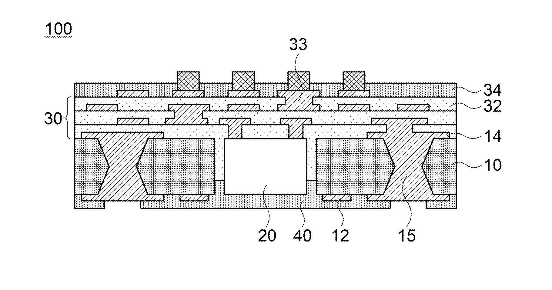
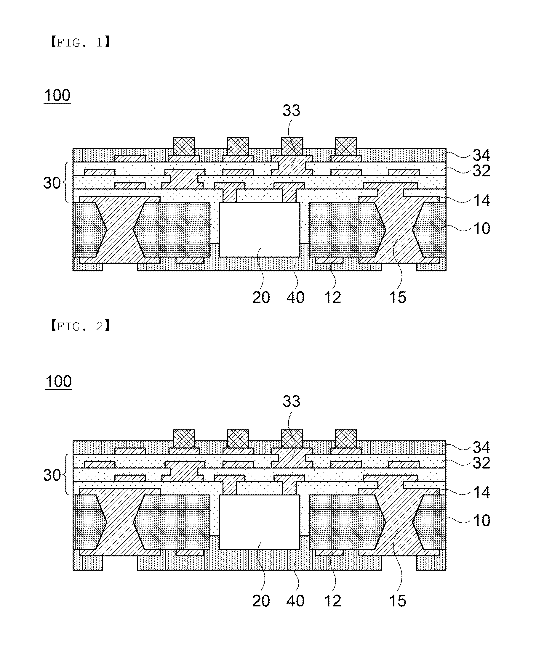
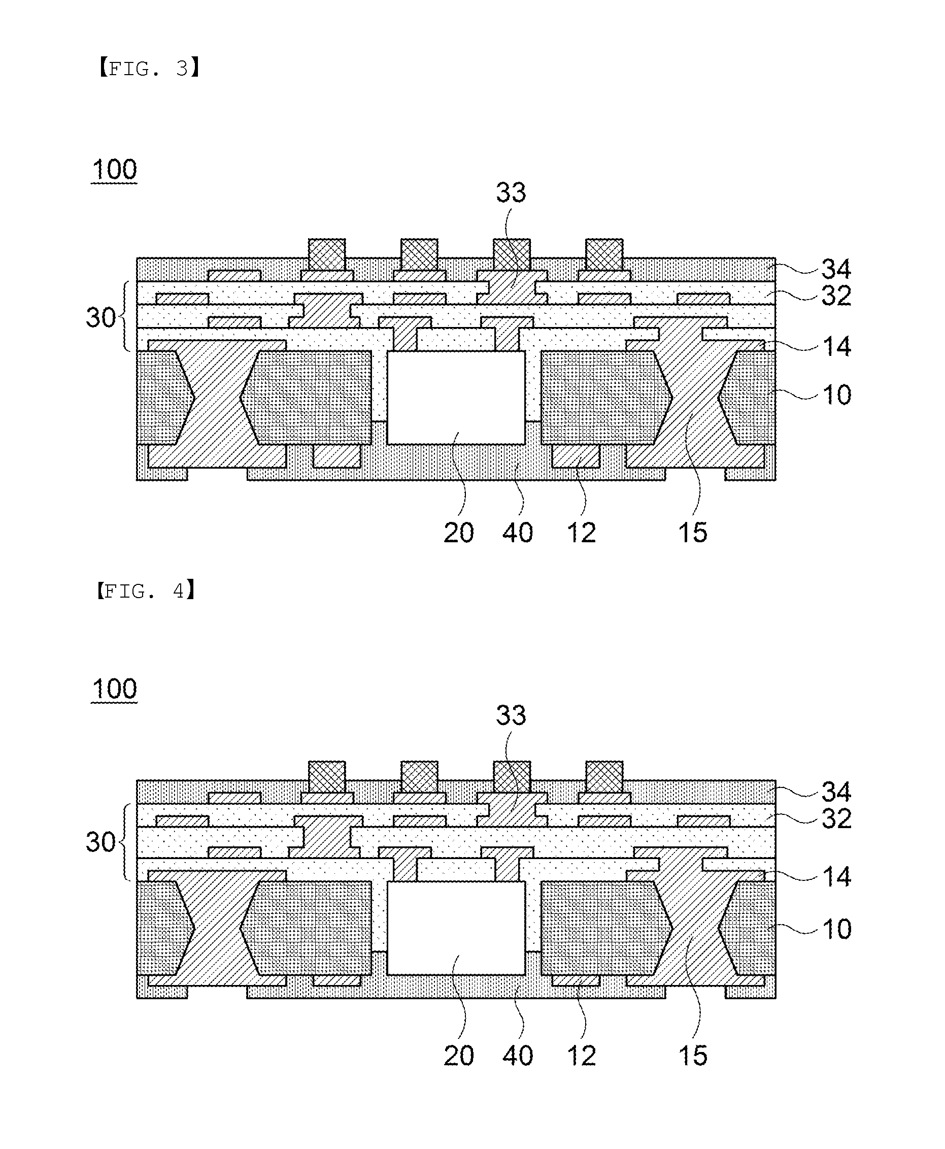
[0029]FIG. 1 is an exemplary view showing a printed circuit board according to an exemplary embodiment of the present invention; FIG. 2 is an exemplary view showing a printed circuit board according to another exemplary embodiment of the present invention; FIG. 3 is an exemplary view showing a state in which a lower pad of a core is formed to have a thickness thicker than that of an upper portion in the printed circuit board according to the exemplary embodiment of the present invention; FIG. 4 is an exemplary view showing a state in which a plurality of layers having different thicknesses from each other are configured in the printed circuit board according to the exemplary embodiment of the present invention; and FIGS. 5A to 5D are exemplary views showing a manufacturing method of a printed circuit board according to the exemplary embodiment of...


PUM

PropertyMeasurementUnit
Thicknessaaaaaaaaaa
aaaaaaaaaa

Abstract

Disclosed herein is a printed circuit board capable of implementing slimness by decreasing the number of entire layers through an asymmetrical build-up structure in which an electric device is embedded, the printed circuit board including: a core layer including a cavity formed therein so that an electric device is embedded and a circuit pattern and a pad formed on upper and lower surfaces thereof; a through via formed in the core layer so as to connect the upper and the lower pads of the core layer to each other; a plurality of insulating layers built-up on the core layer and including a plurality of vias so as to be electrically connected to the through via; and a solder resist layer applied onto a lower portion of the core layer so that a lower surface of the through via is partially exposed.

Description

CROSS REFERENCE(S) TO RELATED APPLICATIONS[0001]This application claims the benefit under 35 U.S.C. Section 119 of Korean Patent Application Serial No. 10-2013-0084775, entitled “Printed Circuit Board and Manufacturing Method Thereof” filed on Jul. 18, 2013, which is hereby incorporated by reference in its entirety into this application.BACKGROUND OF THE INVENTION[0002]1. Technical Field[0003]The present invention relates to a printed circuit board and a manufacturing method thereof, and more particularly, to a printed circuit board capable of implementing slimness by decreasing the entire number of layers through an asymmetrical build-up structure in which an electric device is embedded, and a manufacturing method thereof.[0004]2. Description of the Related Art[0005]In accordance with the trends toward lightness, miniaturization, high-speed, multi-functionality, high performance of electronic products, an embedded printed circuit board (embedded PCB) technology of embedding a devic...

Claims


Application Information

Patent Timeline
IPC IPC(8): H05K1/18H05K3/30H05K3/00H05K1/02H05K1/11
CPCH05K1/0271H05K3/007H05K1/184H05K1/115H05K3/305H05K1/111H05K1/185H05K3/0097H05K3/429H05K3/4602H05K3/4644H05K2201/0187H05K2201/0191H05K2201/0352H05K2201/09136H05K2203/0191H05K2203/1536H01L2924/3511Y10T29/49139H05K3/46
Inventor KIM, SANG HOONMIN, TAE HONGLEE, JUNG HANKIM, HYE JIN
Owner SAMSUNG ELECTRO MECHANICS CO LTD
Why Eureka
Try Eureka