Method of manufacturing a wiring board

a manufacturing method and wiring board technology, applied in the field of wiring board technology, can solve the problems of reducing throughput and cost-effectiveness, imposing restrictions on the design of wiring boards, and complicating the manufacturing process, so as to minimize the warpage of the wiring board structure, and reduce the cost of manufacturing. cost

Active Publication Date: 2012-10-16
IMBERATEK LLC
View PDF17 Cites 4 Cited by
  • Summary
  • Abstract
  • Description
  • Claims
  • Application Information

AI Technical Summary

Benefits of technology

[0011]The manufacturing method according to the present invention enables the fabrication of an essentially symmetrical double-sided structure for the wiring board. In this method the electrical components can be embedded in the wiring board structure while the fabrication of wiring patterns on each side of the structure can be done on an essentially symmetrical double-sided structure, before the step of separating the structural aids, i.e. before separating the individual sides of the double-sided structure. When a symmetrical structure like this goes through heat-treating or annealing, warping of the structure can be minimized as the coefficient of thermal expansion can be made essentially same on each side of the plane of symmetry. This makes the fabrication process relatively simple and also results in a reliable, mechanically and electrically robust, wiring board structure. Additionally the method of the present invention does not impose limitations to the design of the wiring board structure; benefits of the method and of the structure can be obtained as long as the coefficients of thermal expansion are similar on each side of one double-sided structure. The double-sided product according to the present invention may be used e.g. as a base structure and a specific wiring configuration may be processed on each side of this base structure by using e.g. conventional lithography and deposition techniques such as laser patterning, chemical etching, electroless coating, electrolytic deposition or various thin-film deposition techniques such as CVD or PECVD. The fabrication of wiring patterns on each side of the structure can be done before the step of separating the structural aids, i.e. before separating the individual sides of the double-sided structure.
[0012]In one embodiment of the present invention the structural aid is a molding resin sheet, for embedding the electrical component into the slot in the molding resin sheet. When a molding resin sheet is utilized as the structural aid an electrical component can be embedded in a slot conforming to the shape of the component. In this way the material surrounding the electrical component is essentially the same all around the component and the wiring board structure can be made very homogenous resulting in e.g. a very homogenous coefficient for thermal expansion. This further helps minimizing warpage of the wiring board structure. Additional benefits of using a molding resin sheet as the structural aid are reduced mechanical stresses caused by possible temperature changes in the structure, and the ability to use small component-to-component distances which can be used to reduce the width and thickness of a wiring board module. The molding resin sheet also enables a simple wiring board structure and a simple process flow for fabricating the wiring board.
[0017]Confining the bonding of the structural layers on each side of the planar temporary bonding means to a peripheral portion (region) around this bonding means facilitates the separation of the structural layers and thereby the structural aids on each side of the planar temporary bonding means from each other.
[0020]The method according to the present invention enables a wiring board structure in which an electrical component is embedded in the structure formed by the structural layer and / or by the at least one structural aid, and is electrically connected to the conductors on the surface of the structure. This embedded structure enhances the mechanical stability of the wiring board, and provides protection for the embedded electrical components from environment. An embedded structure furthermore enables reducing the final thickness of an assembled wiring board structure. Another advantage of the method according to the present invention is that it does not require developing new processing equipment but the method may be carried out in many existing production lines with minor modifications to the hardware.

Problems solved by technology

A common problem with wiring boards is warping as a result of the manufacturing process.
A problem with prior-art approaches, including the aforementioned publications, in reducing warping of the wiring board is that they impose restrictions on the design of wiring boards.
Another problem with solutions of the prior art is that they complicate the manufacturing process and thereby decrease its throughput and cost-effectiveness.
Reduced flexibility in the design of wiring boards may also compromise the reliability of electrical connections in the wiring board.

Method used


Image

  • Method of manufacturing a wiring board
  • Method of manufacturing a wiring board
  • Method of manufacturing a wiring board

Examples


first embodiment

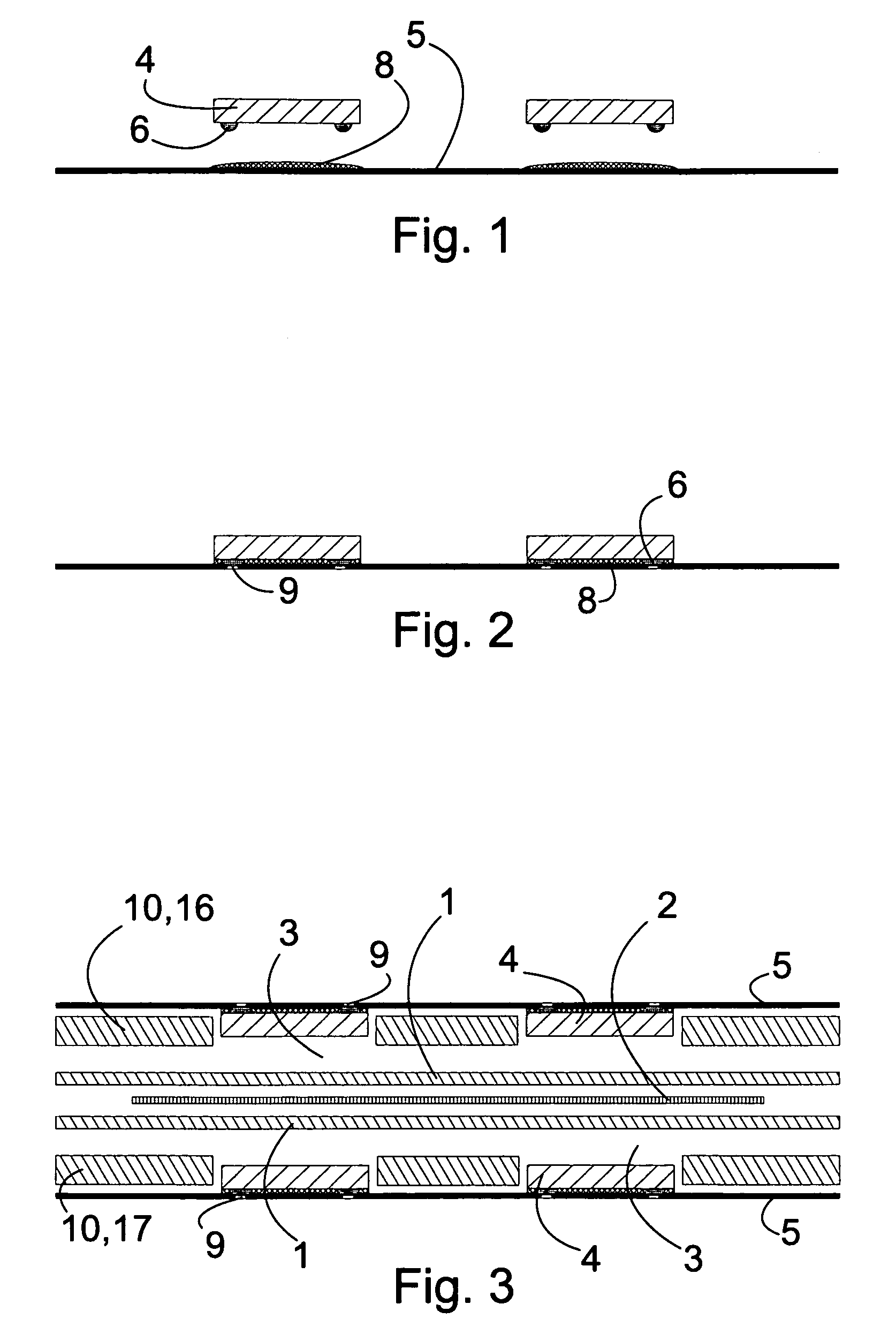
[0023]FIG. 1 is a first view of a schematic illustration of a method according to the present invention,

[0024]FIG. 2 is a second view of a schematic illustration of a method according to a first embodiment of the present invention,

[0025]FIG. 3 is a third view of a schematic illustration of a method according to a first embodiment of the present invention,

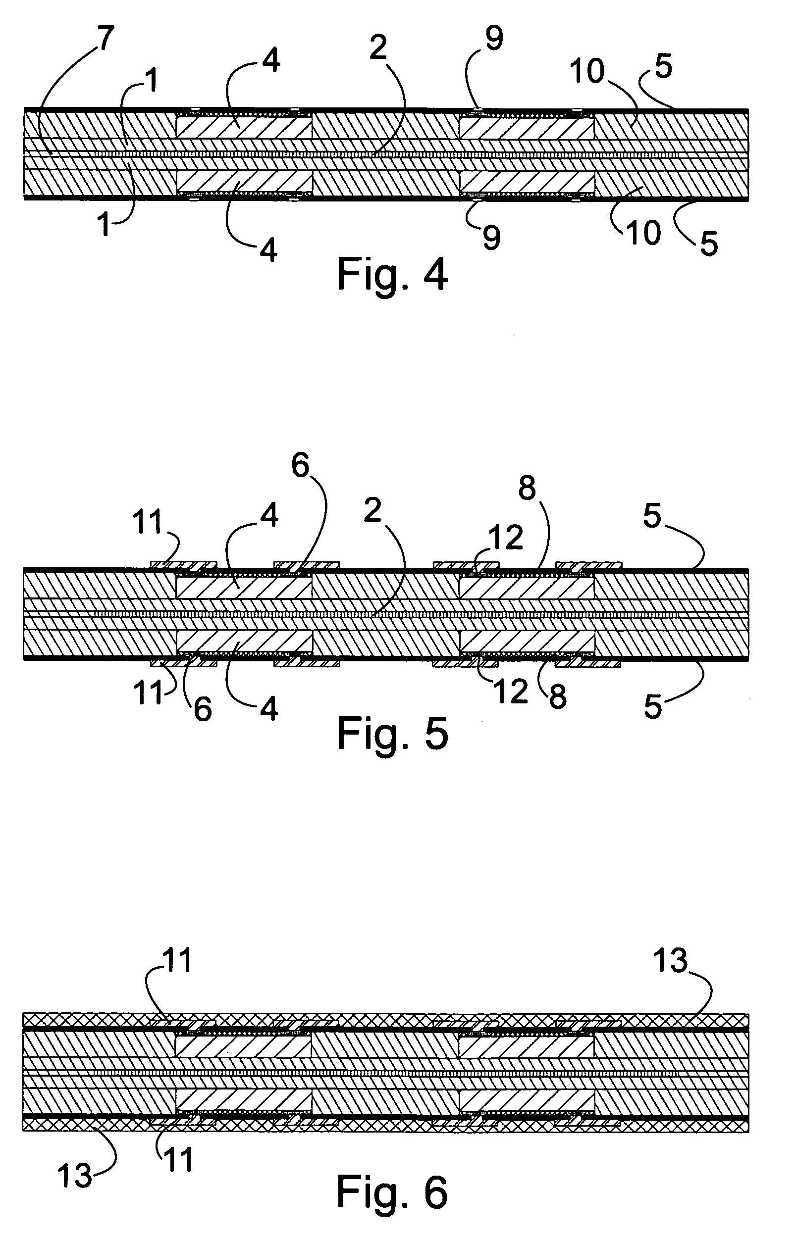
[0026]FIG. 4 is a fourth view of a schematic illustration of a method according to a first embodiment of the present invention,

[0027]FIG. 5 is a fifth view of a schematic illustration of a method according to a first embodiment of the present invention,

[0028]FIG. 6 is a sixth view of a schematic illustration of a method according to a first embodiment of the present invention,

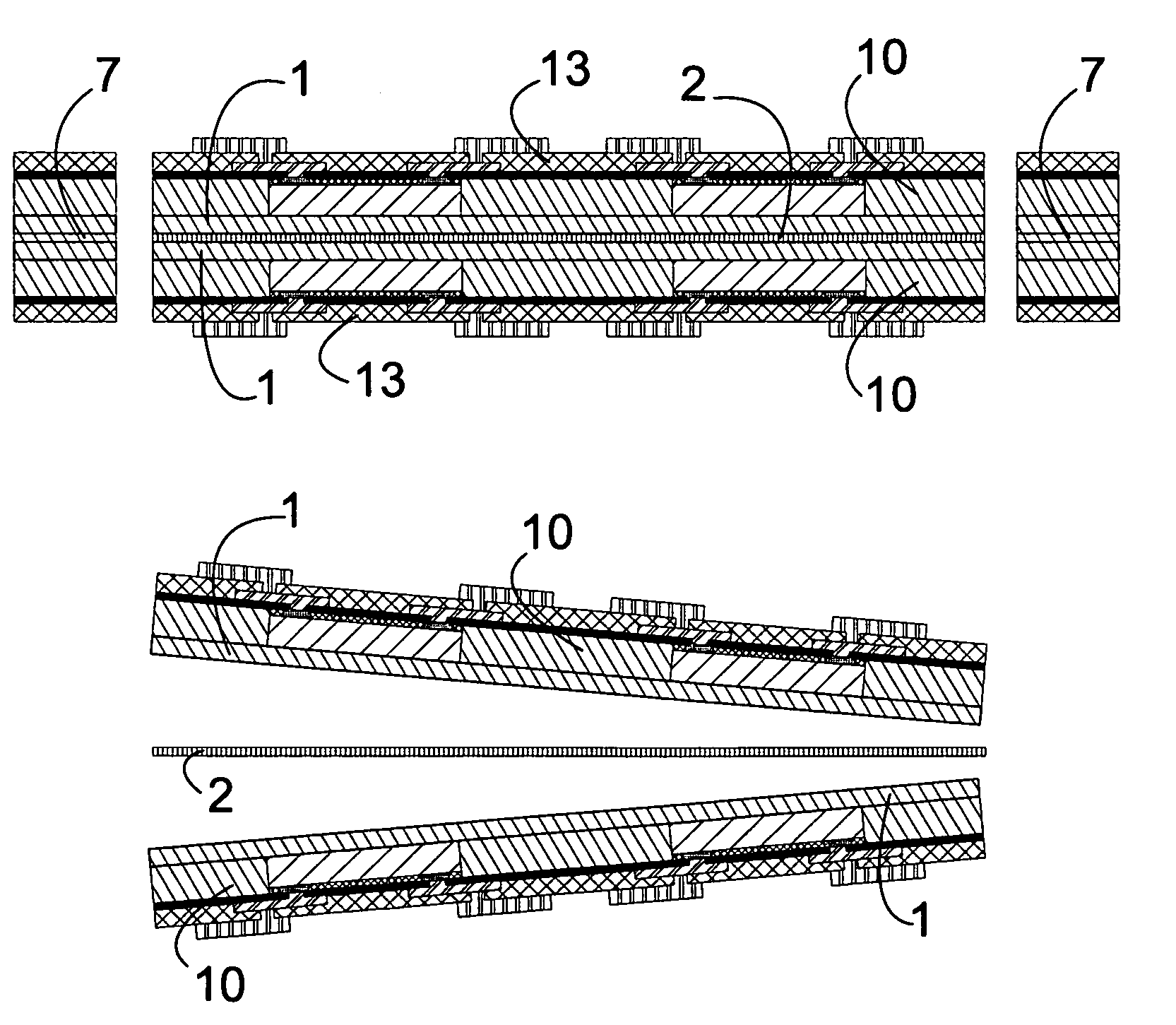
[0029]FIG. 7 is a seventh view of a schematic illustration of a method according to a first embodiment of the present invention,

[0030]FIG. 8 is an eighth view of a schematic illustration of a method according to a first embodiment of the present invention,

[0031...

second embodiment

[0032]FIG. 10 is a first view of a schematic illustration of a method according to the present invention,

[0033]FIG. 11 is a second view of a schematic illustration of a method according to a second embodiment of the present invention,

[0034]FIG. 12 is a third view of a schematic illustration of a method according to a second embodiment of the present invention,

[0035]FIG. 13 is a fourth view of a schematic illustration of a method according to a second embodiment of the present invention,

[0036]FIG. 14 is a fifth view of a schematic illustration of a method according to a second embodiment of the present invention,

[0037]FIG. 15 is a sixth view of a schematic illustration of a method according to a second embodiment of the present invention,

[0038]FIG. 16 is a seventh view of a schematic illustration of a method according to a second embodiment of the present invention,

[0039]FIG. 17 is an eighth view of a schematic illustration of a method according to a second embodiment of the present ...

third embodiment

[0041]FIG. 19a is a first view of a schematic illustration of a method according to the present invention,


PUM

PropertyMeasurementUnit
surface areaaaaaaaaaaa
electricalaaaaaaaaaa
packaging densityaaaaaaaaaa

Abstract

A method for manufacturing a wiring board, comprising the steps of mounting at least one structural aid on each side of a planar temporary bonding means, arranging a slot from the at least one structural aid on each side of the planar temporary bonding means, embedding the electrical component in the slot, such that the terminals of the electrical component face away from the planar temporary bonding means, mounting at least one electrical component on a component foil, such that the terminals of the electrical component face the component foil, mounting the component foil at least partially on the at least one structural aid, on each side of the planar temporary bonding means.

Description

[0001]This application claims benefit of Serial No. 20085332, filed 18 Apr. 2008 in Finland and which application is incorporated herein by reference. To the extent appropriate, a claim of priority is made to the above disclosed application.FIELD OF THE INVENTION[0002]The present invention relates to wiring board technology. Especially the present invention relates to a wiring board and a method for manufacturing a wiring board with an electrical component, using a planar temporary bonding means.BACKGROUND OF THE INVENTION[0003]Important aspects of state-of-the-art wiring boards and methods for their manufacturing include dense mounting of semiconductor chips enabling small lateral and vertical dimensions, and robustness including reliable electrical contacts and flatness to ensure good alignment of features during lithographic processing. Furthermore the production process to manufacture the wiring boards should be as cost-effective as possible especially in mass production. This c...

Claims


Application Information

Patent Timeline
Patent Type & Authority Patents(United States)
IPC IPC(8): H05K3/30
CPCH01L21/561H01L21/6835H01L23/3121H01L24/19H01L25/0652H01L25/50H05K1/185H05K1/188H05K3/0097H01L21/568Y10T29/49117H01L24/90H01L2221/68345H01L2224/04105H01L2224/20H01L2224/2919H01L2224/83192H01L2224/90H01L2224/92144H01L2924/01029H01L2924/01033H01L2924/01046H01L2924/01075H01L2924/01078H01L2924/01082H05K1/189H05K3/0052H05K2201/10674H05K2203/1469H05K2203/1536Y10T29/49146Y10T29/49144Y10T29/4913H01L2924/1461H01L2924/12041H01L2924/01006H01L2224/73267H01L2924/0665H01L2924/00H01L2924/18162H01L2924/181H01L2224/92244H01L2924/3511H05K1/18H05K3/46
Inventor PALM, PETTERIKUJALA, ARNI
Owner IMBERATEK LLC
Why Eureka
Try Eureka