Electronics component embedded PCB

a technology of electronic components and printed circuit boards, applied in the direction of printed circuits, printed circuits, printed electric components, etc., can solve the problems of essentially limited critical thickness for preventing warpage, inability to embed electronic components having a certain thickness or less, and etc., to achieve the effect of reducing the chance of warpag

Inactive Publication Date: 2013-12-31
SAMSUNG ELECTRO MECHANICS CO LTD
View PDF13 Cites 2 Cited by
  • Summary
  • Abstract
  • Description
  • Claims
  • Application Information

AI Technical Summary

Benefits of technology

[0008]The present invention provides an electronic component embedded printed circuit board and a manufacturing method thereof, in which the printed circuit board is formed in a symmetrical structure considering the coefficients of thermal expansion in order to minimize the warpage that is caused by mounting an electronic component while making the printed circuit board thinner.

Problems solved by technology

It is also impossible to embed an electronic component having a certain thickness or less because the warpage of a board occurs in a direction in which the electronic component is embedded under thermal stresses.
Moreover, since a stacking material that is used for printed circuit boards can not be manufactured to be thinner than a certain thickness because of electrical insulation, a critical thickness for preventing the warpage is essentially limited due to the properties of the material.
In a conventional printed circuit board, since the locations and thicknesses of electronic components embedded therein are asymmetric with respect to the entire thickness or shape, it is under repeated thermal stresses, particularly thermal stresses in a process, such as soldering, performed at temperatures above 200° C., and thus there is a chance of warpage.
Due to the warpage effect, an electronic component generally has to be maintained to a certain thickness or greater, and thus the entire electronic component embedded printed circuit board becomes inevitably thicker.

Method used


Image

  • Electronics component embedded PCB
  • Electronics component embedded PCB
  • Electronics component embedded PCB

Examples


Embodiment Construction

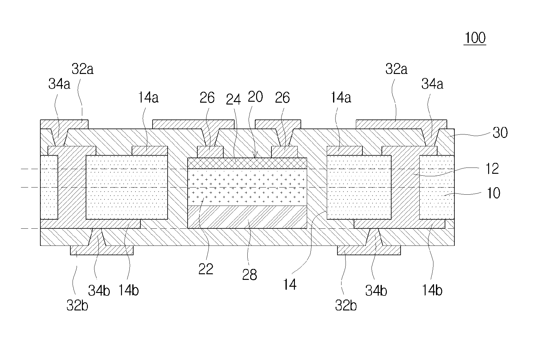
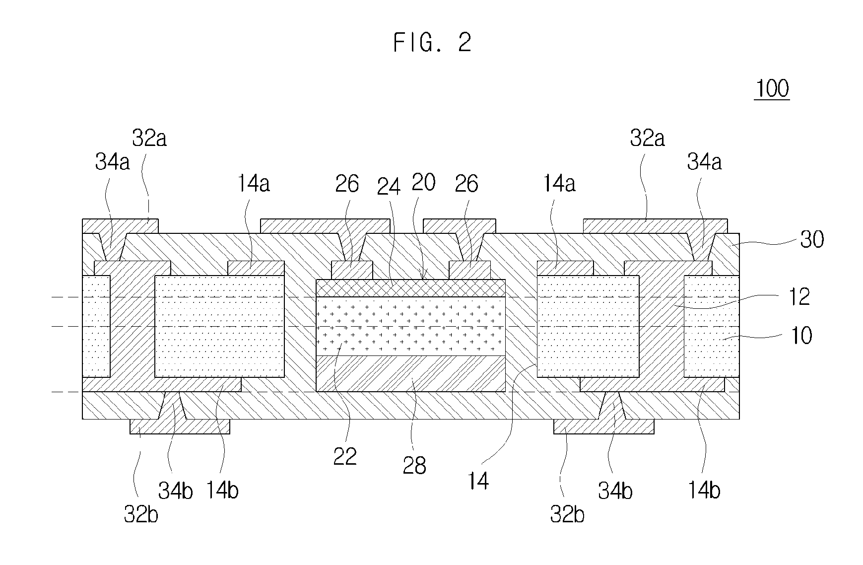
[0015]As the invention allows for various changes and numerous embodiments, particular embodiments will be illustrated in the drawings and described in detail in the written description. However, this is not intended to limit the present invention to particular modes of practice, and it is to be appreciated that all changes, equivalents, and substitutes that do not depart from the spirit and technical scope of the present invention are encompassed in the present invention. In the description of the present invention, certain detailed explanations of related art are omitted when it is deemed that they may unnecessarily obscure the essence of the invention.

[0016]An electronic component embedded printed circuit board according to certain embodiments of the present invention will be described below in more detail with reference to the accompanying drawings. Those components that are the same or are in correspondence are rendered the same reference numeral regardless of the figure number...


PUM


Abstract

An electronic component embedded printed circuit board is disclosed. In accordance with an embodiment of the present invention, the electronic component embedded printed circuit board is a printed circuit board in which an electronic component is embedded in a core board, and the electronic component includes a silicon layer and a passivation layer, which is formed on one surface of the silicon layer. Here, a center line of the silicon layer and a center line of the core board are placed on a same line.

Description

CROSS-REFERENCE TO RELATED APPLICATIONS[0001]This application claims the benefit of Korean Patent Application No. 10-2009-0103766, filed with the Korean Intellectual Property Office on Oct. 29, 2009, the disclosure of which is incorporated herein by reference in its entirety.BACKGROUND[0002]1. Technical Field[0003]The present invention is related to an electronic component embedded printed circuit board.[0004]2. Description of the Related Art[0005]As part of the next generation versatile compact package technology, the development of electronic component embedded printed circuit boards is recently receiving attention. The electronic component embedded printed circuit board also includes a high functional aspect, in addition to the advantages of versatility and compactness. This is because it can provide a solution to improve the reliability problem that may occur in the electrical connection between electronic components using wire bonding or soldering that is used in a flip chip or...

Claims


Application Information

Patent Timeline
Patent Type & Authority Patents(United States)
IPC IPC(8): H05K1/16
CPCH01L2924/01033H01L24/24H01L2924/1517H01L2224/24227H01L23/3121H01L2924/014H05K1/185H01L2924/01006H01L2924/15153H05K1/0271H05K3/4602H05K2201/10674H01L23/5389H01L2224/04105H01L2924/351H01L2924/3511H01L2924/00H05K1/18H05K3/30
Inventor BYUN, JUNG-SOOCHUNG, YUL-KYOPARK, HWA-SUNLEE, KYUNG-MINKIM, MIKELEE, DOO-HWAN
Owner SAMSUNG ELECTRO MECHANICS CO LTD
Why Eureka
Try Eureka