
Finfet with electrically isolated active region on bulk semiconductor substrate and method of fabricating same

a technology of active region and semiconductor substrate, which is applied in the direction of transistors, semiconductor devices, electrical equipment, etc., can solve the problems of increasing static power consumption, increasing variability, and leaking path from source to drain

Active Publication Date: 2015-01-22
GLOBALFOUNDRIES US INC
View PDF2 Cites 60 Cited by
  • Summary
  • Abstract
  • Description
  • Claims
  • Application Information

AI Technical Summary

Benefits of technology

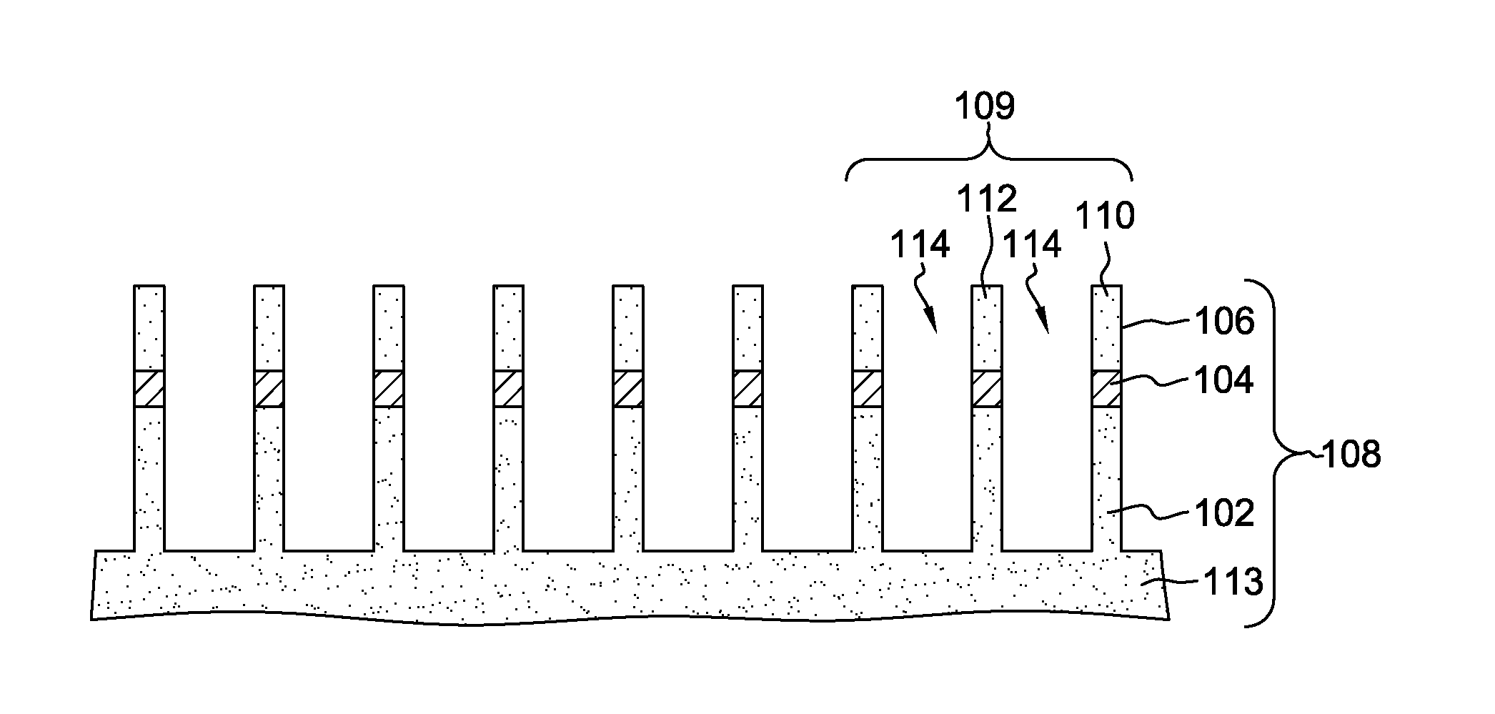
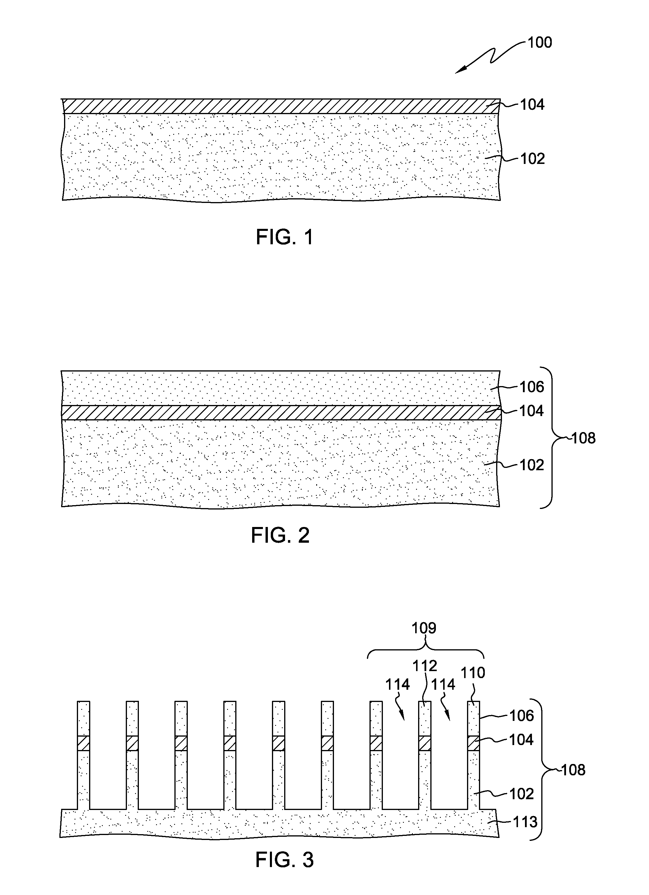
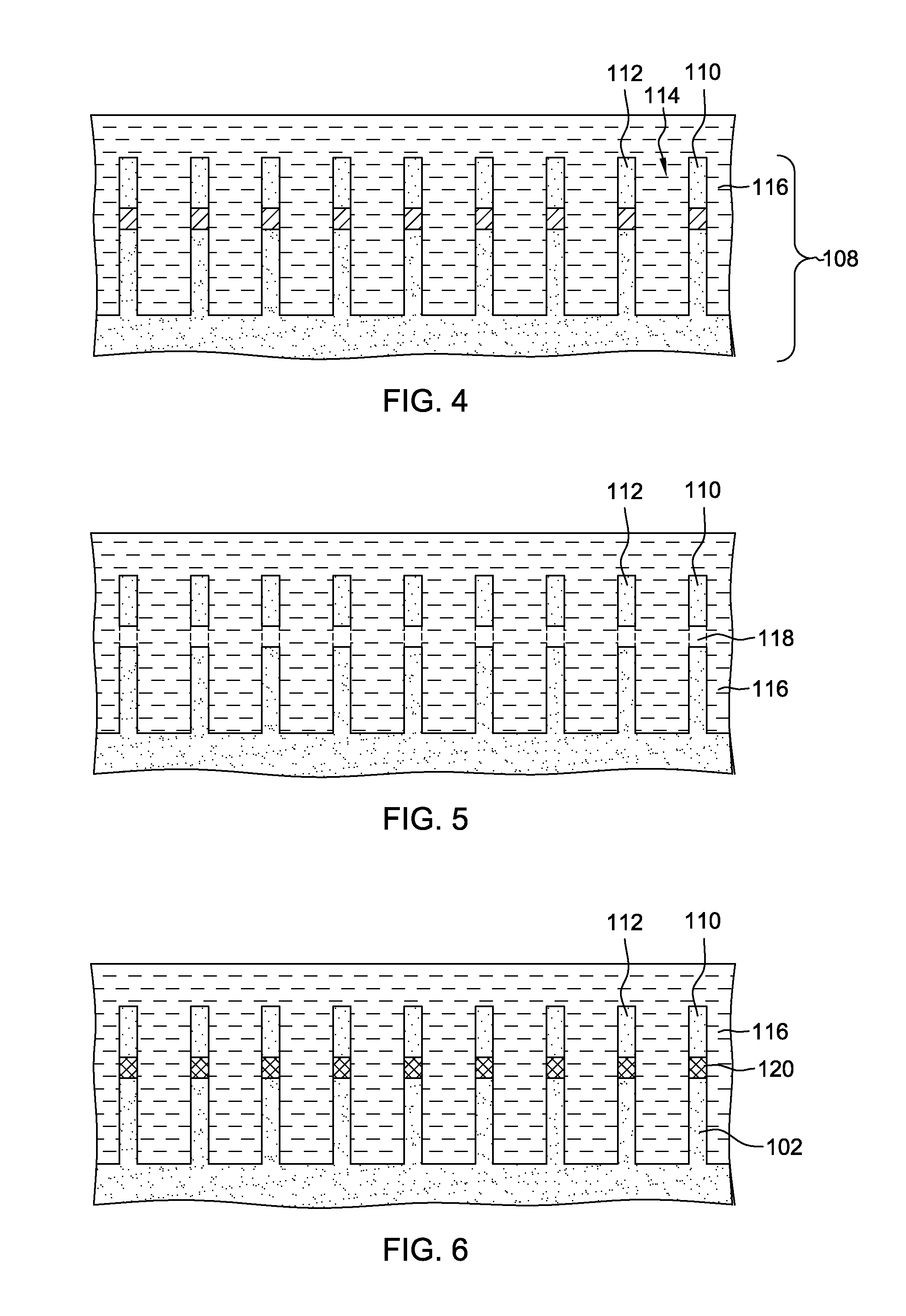
The present invention provides a method for electrically isolating the active region of a fin in a finFET from the inactive region below, by converting a sacrificial layer to a dielectric layer. The invention also provides a semiconductor stack including a semiconductor substrate and at least one fin with an active region, an inactive region, and a separation region, each region including at least one dielectric material. The invention also provides a transistor including a bulk semiconductor substrate and at least one fin with a channel region, directly below which is a second region including at least one dielectric material and a third region coupled to the substrate. This improves device performance and stability.

Problems solved by technology

However, a problem with bulk FinFET devices is that a leakage path from source to drain exists through a portion of the fin not covered by the gate, but lies below the channel.
The leakage of current from source to drain through the lower (un-gated) part of the fin, commonly known as punch-through leakage, causes an increase of static power consumption which is undesirable in modern submicron devices.
However, the impurities doped by the punch-through-stopper (PTS) implantation may diffuse into the channel region, increasing the variability due to random dopant fluctuation (RDF) and lowering the carrier mobility of the channel region.

Method used


Image

  • Finfet with electrically isolated active region on bulk semiconductor substrate and method of fabricating same
  • Finfet with electrically isolated active region on bulk semiconductor substrate and method of fabricating same
  • Finfet with electrically isolated active region on bulk semiconductor substrate and method of fabricating same

Examples


Embodiment Construction

[0017]Aspects of the present invention and certain features, advantages, and details thereof, are explained more fully below with reference to the non-limiting examples illustrated in the accompanying drawings. Descriptions of well-known materials, fabrication tools, processing techniques, etc., are omitted so as not to unnecessarily obscure the invention in detail. It should be understood, however, that the detailed description and the specific examples, while indicating aspects of the invention, are given by way of illustration only, and are not by way of limitation. Various substitutions, modifications, additions, and / or arrangements, within the spirit and / or scope of the underlying inventive concepts will be apparent to those skilled in the art from this disclosure.

[0018]Approximating language, as used herein throughout the specification and claims, may be applied to modify any quantitative representation that could permissibly vary without resulting in a change in the basic fun...


PUM


Abstract

A semiconductor stack of a FinFET in fabrication includes a bulk silicon substrate, a selectively oxidizable sacrificial layer over the bulk substrate and an active silicon layer over the sacrificial layer. Fins are etched out of the stack of active layer, sacrificial layer and bulk silicon. A conformal oxide deposition is made to encapsulate the fins, for example, using a HARP deposition. Relying on the sacrificial layer having a comparatively much higher oxidation rate than the active layer or substrate, selective oxidization of the sacrificial layer is performed, for example, by annealing. The presence of the conformal oxide provides structural stability to the fins, and prevents fin tilting, during oxidation. Selective oxidation of the sacrificial layer provides electrical isolation of the top active silicon layer from the bulk silicon portion of the fin, resulting in an SOI-like structure. Further fabrication may then proceed to convert the active layer to the source, drain and channel of the FinFET. The oxidized sacrificial layer under the active channel prevents punch-through leakage in the final FinFET structure.

Description

BACKGROUND OF THE INVENTION[0001]1. Technical Field[0002]The present invention generally relates to semiconductor transistors. More particularly, the present invention relates to fabricating a FinFET on a bulk semiconductor substrate with a dielectric layer directly under the active region.[0003]2. Background Information[0004]Fin field-effect transistors (FinFET) devices have been developed to replace conventional planar bulk MOSFETs in advanced CMOS technology due to their improved short-channel effect immunity and Ion / Ioff ratio. However, a problem with bulk FinFET devices is that a leakage path from source to drain exists through a portion of the fin not covered by the gate, but lies below the channel. The leakage of current from source to drain through the lower (un-gated) part of the fin, commonly known as punch-through leakage, causes an increase of static power consumption which is undesirable in modern submicron devices.[0005]In one solution, punch-through leakage in submicr...

Claims


Application Information

Patent Timeline
IPC IPC(8): H01L29/66H01L29/78
CPCH01L29/66795H01L29/785H01L21/76224
Inventor AKARVARDAR, MURAT KEREMFRONHEISER, JODY A.JACOB, AJEY POOVANNUMMOOTTIL
Owner GLOBALFOUNDRIES US INC
Learn More