Light emitting device and method of manufacturing light emitting device

a technology of light emitting device and light emitting chromaticity, which is applied in the direction of semiconductor devices, semiconductor/solid-state device details, electrical devices, etc., can solve the problems of product not meeting the deviation of light emission chromaticity, and achieves the effect of not being normally of commercial value for products that do not meet the prescribed light emission chromaticity rang

Active Publication Date: 2015-01-29
NICHIA CORP
View PDF7 Cites 35 Cited by
  • Summary
  • Abstract
  • Description
  • Claims
  • Application Information

AI Technical Summary

Benefits of technology

[0008]The present invention is proposed in relation to the problems above, and has the object of providing a light emitting device that adjusts light emission chromaticity by use of a different principle to the principle used in the prior art, and to a manufacturing method for a light emitting device that adjusts light emission chromaticity by use of a different pr

Problems solved by technology

Manufacturing processes for such light emitting devices result in a deviation in the light emission chromaticity as a result in a deviation or the like in the content or particle diameter of the fluorescent su

Method used


Image

  • Light emitting device and method of manufacturing light emitting device
  • Light emitting device and method of manufacturing light emitting device
  • Light emitting device and method of manufacturing light emitting device

Examples


first embodiment

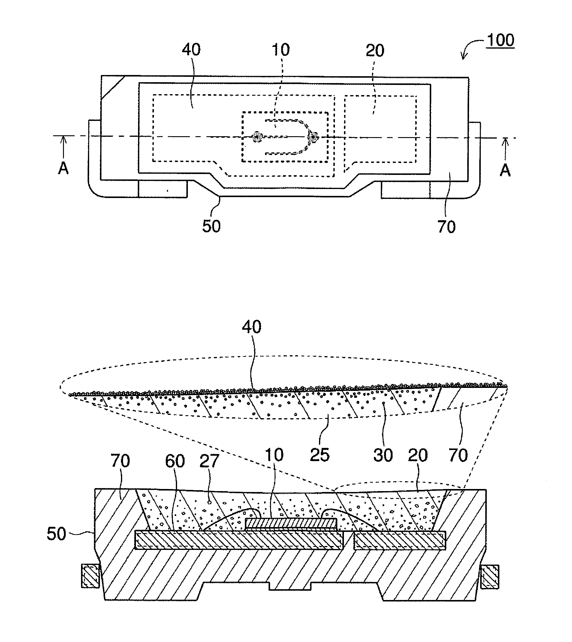
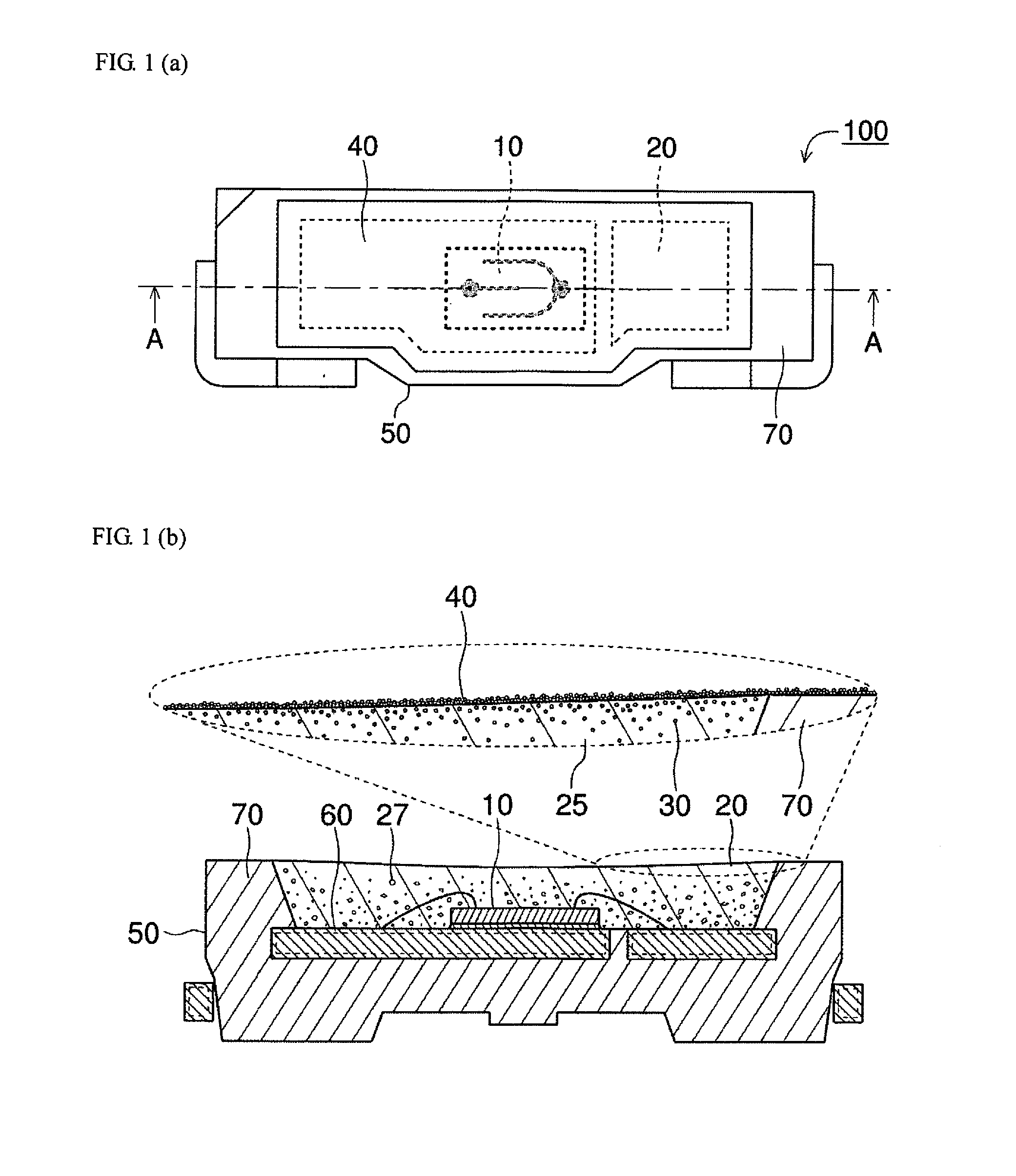
[0036]FIG. 1(a) is a schematic upper view of a light emitting device according to a first embodiment, and 1(b) is a schematic sectional view along the sectional face A-A.

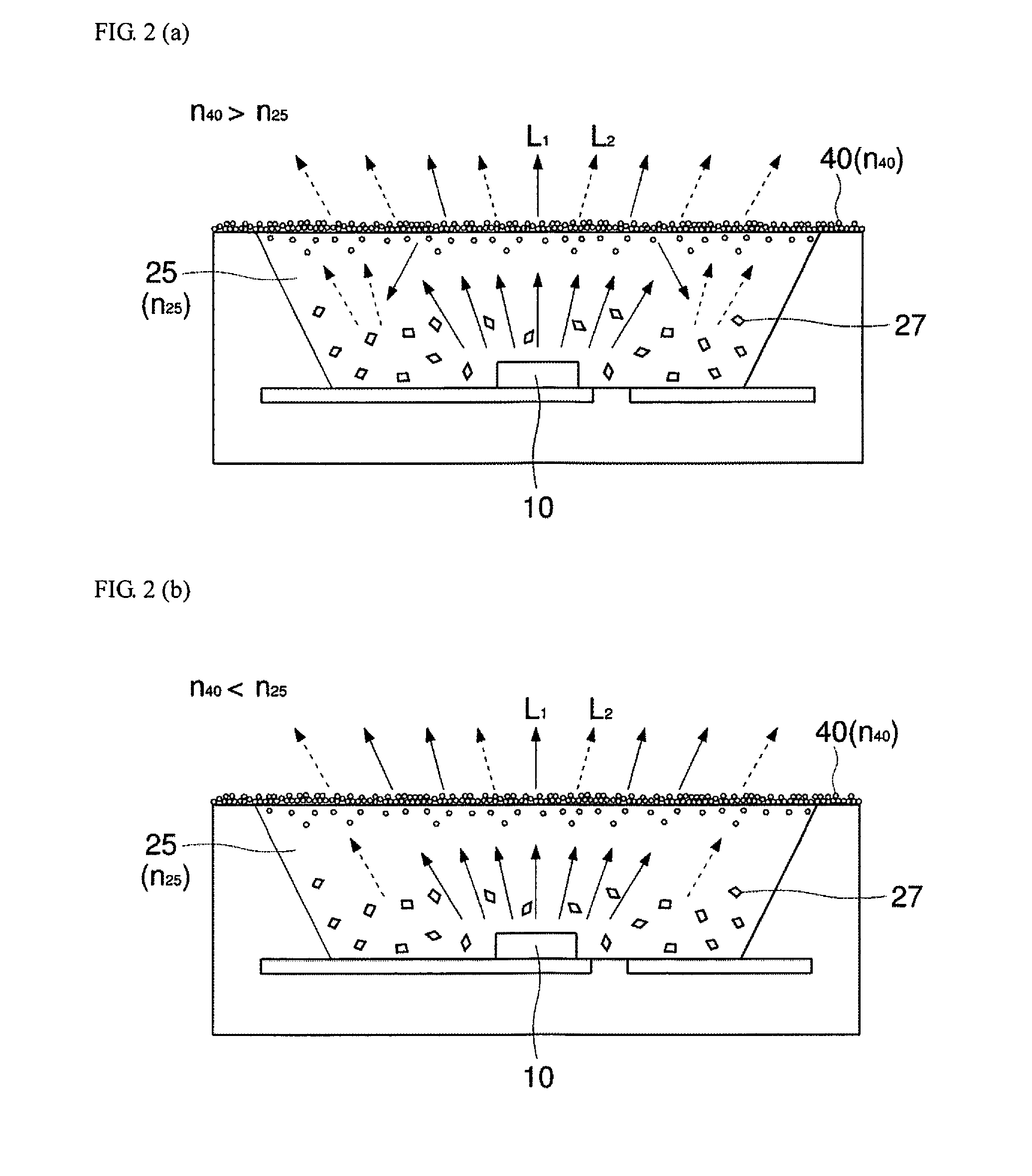
[0037]As illustrated in FIG. 1, the light emitting device 100 includes a light emitting element 10, a translucent member 20, and a film 40. Furthermore, the light emitting device 100 includes a mounting base 50 configured to mount the light emitting element 10. The mounting base 50 includes an enclosure body 70. The light emitting element 10 emits visible light. The translucent member 20 includes a translucent base material 25. The translucent member 20 includes a fluorescent substance 27, and is provided on the light emitting element 10. The fluorescent substance 27 emits visible light when excited by light emitted from the light emitting element 10. The film 40 is provided on the upper surface of the translucent member 20. The film 40 is configured as an agglutination of nanoparticles 30 that exhibit a different r...

second embodiment

[0059]FIG. 4 is a schematic sectional view of a light emitting device according to a second embodiment. As illustrated in FIG. 4, the light emitting device 200 includes a light emitting element 11, a translucent member 21, and a film 40. The light emitting device 200 does not include a mounting base configured to mount the light emitting element 10. The light emitting device 200 is termed a chip size package (CSP), or the like. The light emitting device 200 includes an enclosure body 71 that is configured to enclose a light emitting element 11. The enclosure body 71 is provided in contact with the lower and the lateral sides of the light emitting element 11. Furthermore, the light emitting device 200 includes a projecting electrode 80 that is connected to the light emitting element 11. The light emitting element 11 emits visible light. The translucent member 21 includes a translucent base material 25. The translucent member 21 includes a fluorescent substance 27, and is provided on ...

third embodiment

[0062]FIG. 5 is a schematic sectional view of a light emitting device according to a third embodiment. As illustrated in FIG. 5, the light emitting device 250 includes a light emitting element 12, a translucent member 21, and a film 40. The light emitting device 250 does not include a mounting base configured to mount the light emitting element 10 and an enclosure body. The light emitting device 250 is also termed a chip size package (CSP), or the like. The light emitting device 250 includes a projecting electrode 80 that is connected to the light emitting element 12. The light emitting element 12 emits visible light. The translucent member 21 includes a translucent base material 25. The translucent member 21 includes a fluorescent substance 27, and is provided on the light emitting element 12. The fluorescent substance 27 emits visible light when excited by light emitted from the light emitting element 12. The film 40 is provided on the upper surface of the translucent member 21. T...


PUM


Abstract

A light emitting device includes a light emitting element configured to emit visible light; a fluorescent substance excited by light from the light emitting element and configured to emit visible light; a translucent member containing a translucent base material, which provided on the fluorescent substance or configured to contain the fluorescent substance, and provided on the light emitting element; and a film provided on an upper surface of the translucent member, and configured as an agglutination of nanoparticles having a different refractive index from the base material.

Description

CROSS-REFERENCE TO RELATED APPLICATIONS[0001]This application claims priority to Japanese Patent Application No. 2013-155013 filed on Jul. 25, 2013. The entire disclosure of Japanese Patent Application No. 2013-155013 is hereby incorporated herein by reference.BACKGROUND[0002]1. Technical Field[0003]The present disclosure relates to a light emitting device and a method of manufacturing the light emitting device, and particularly to a light emitting device having a light emitting element and. a method of manufacturing the same.[0004]2. Related Art[0005]In recent years, light emitting devices such as light emitting diodes or the like include a light emitting element that is configured to emit a primary light and a fluorescent substance that is configured to be excited by the primary light and thereby emit a secondary light having a wavelength that is different from the primary light. Another configuration of a light emitting device is provided with a plurality of light emitting elemen...

Claims


Application Information

Patent Timeline
IPC IPC(8): H01L33/50H01L33/58
CPCH01L33/58H01L33/504H01L2933/0091H01L2224/32245H01L2224/48247H01L2224/48257H01L2224/73265H01L33/56H01L2924/00H01L33/50H01L33/52H01L21/02565H01L23/28H01L21/02601H10K50/854H10K50/858H10K59/38
Inventor ABE, KOJIKURAMOTO, MASAFUMIHAYASHI, MASAKI
Owner NICHIA CORP
Why Eureka
Try Eureka