Light emitting apparatus and method for manufacturing thereof

a technology light emitting device, which is applied in the manufacture of electrode systems, electric discharge tubes/lamps, discharge tubes luminescnet screens, etc., can solve the problems of performance degradation of light emitting apparatus, loss of color emission intensity balance, and difficulty in implementing ideal so as to prevent performance decline and degradation, improve color reproducibility and brightness, and reduce the influence of light scattering

Inactive Publication Date: 2013-08-20
SHARP KK
View PDF164 Cites 13 Cited by
  • Summary
  • Abstract
  • Description
  • Claims
  • Application Information

AI Technical Summary

Benefits of technology

[0011]An object of the present invention is to implement a light emitting apparatus that utilizes the characteristics of a nanocrystalline phosphor and is still less prone to suffer from phosphor performance decline and degradation.
[0022]In accordance with an aspect of the present invention, a light emitting apparatus of a long lifetime that utilizes the characteristics of a nanocrystalline phosphor and prevents performance decline and degradation can be implemented. In accordance with another aspect, a light emitting apparatus capable of exhibiting improved color reproducibility and brightness can be implemented in a simple manner. In accordance with still another aspect, a light emitting apparatus capable of adjusting emission color, alleviating influence of light scattering, and less prone to suffer from reduced luminous efficiency or deterioration of the light emitting apparatus can be implemented in a simple manner.

Problems solved by technology

The nanocrystalline phosphor is potentially susceptible to oxygen and moisture, and a resultant problem is therefore that the uppermost-layer phosphor which is in direct contact with the air is degraded to cause the performance of the light emitting apparatus to be deteriorated.
Accordingly, the balance between respective emission intensities of the colors is lost, which makes it difficult to implement ideal color reproducibility and brightness.
Further, the heat radiated from the light emitting device is not sufficiently dissipated from the inside of the light emitting apparatus.
Consequently, the electrical energy may not be converted into optical energy, the luminous efficiency may be reduced and the light emitting apparatus may further be deteriorated.

Method used


Image

  • Light emitting apparatus and method for manufacturing thereof
  • Light emitting apparatus and method for manufacturing thereof
  • Light emitting apparatus and method for manufacturing thereof

Examples


first embodiment

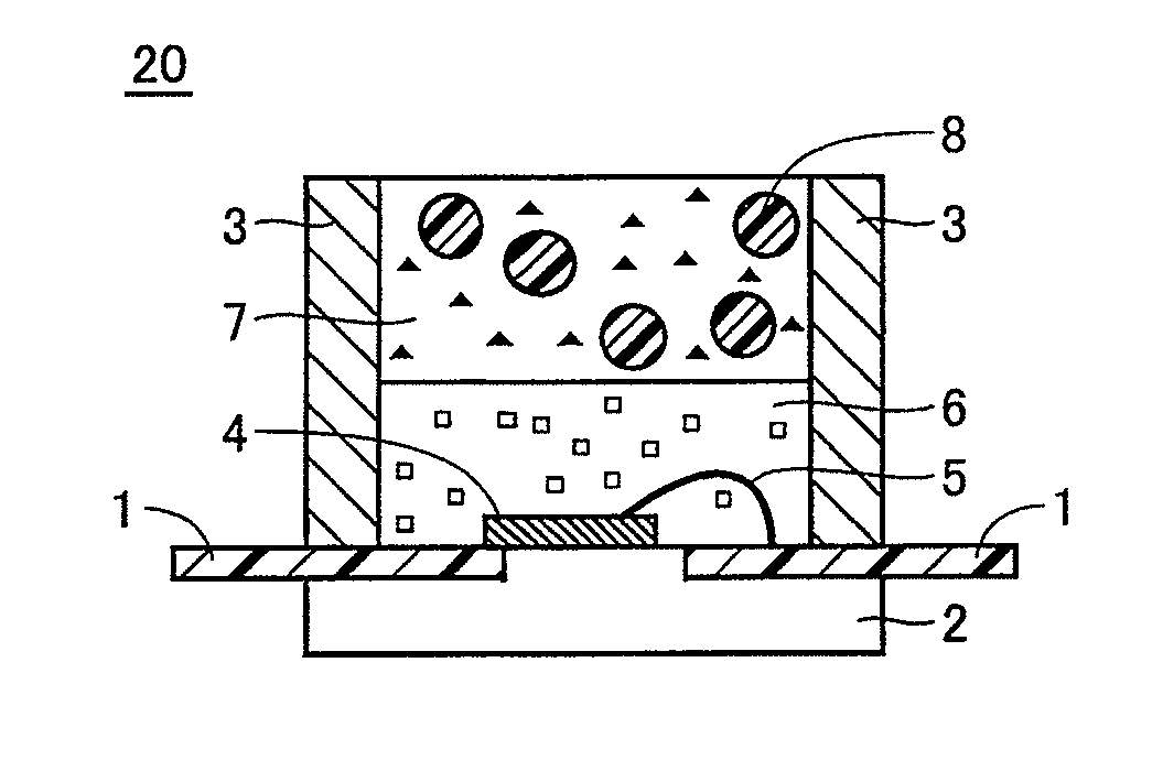
[0038]FIG. 1 is a cross section of a light emitting apparatus in the present embodiment. Light emitting apparatus 10 is constituted of a substrate 2 on which an electrode 1 is formed, a package 3 and a light emitting device 4 that are mounted on electrode 1, a wire 5 connecting light emitting device 4 and electrode 1, and a wavelength conversion unit. The wavelength conversion unit includes a first wavelength conversion unit 6 containing semiconductor nanoparticles and a second wavelength conversion unit 7 containing Eu-activated β-sialon phosphor that are stacked in order of propagation of light from light emitting device 4.

[0039]Electrode 1 is electrically connected by wire 5 to light emitting device 4. As the conductor that forms electrode 1, a material serving as an electrical conduction path for electrical connection with light emitting device 4 has to be used. Specifically, a metallized layer containing particles of a metal such as W, Mo, Cu, or Ag for example may be used. Sub...

second embodiment

[0057]Then, by a similar method to the first embodiment, three different light emitting apparatuses are fabricated in which respective contents of the Eu-activated β-sialon contained in the second wavelength conversion unit are different. More specifically, three different light emitting apparatuses are produced in which respective amounts of Eu-activated β-sialon phosphor per 1 g of the silicone resin (SCR1011) in second wavelength conversion unit 7 are (a) 0.03 g, (b) 0.1 g, and (c) 0.3 g. As the silicone resin, SCR1011, which is the same as the first embodiment, is used and stacked to a thickness which is substantially identical to that of the second wavelength conversion unit shown in FIG. 1.

third embodiment

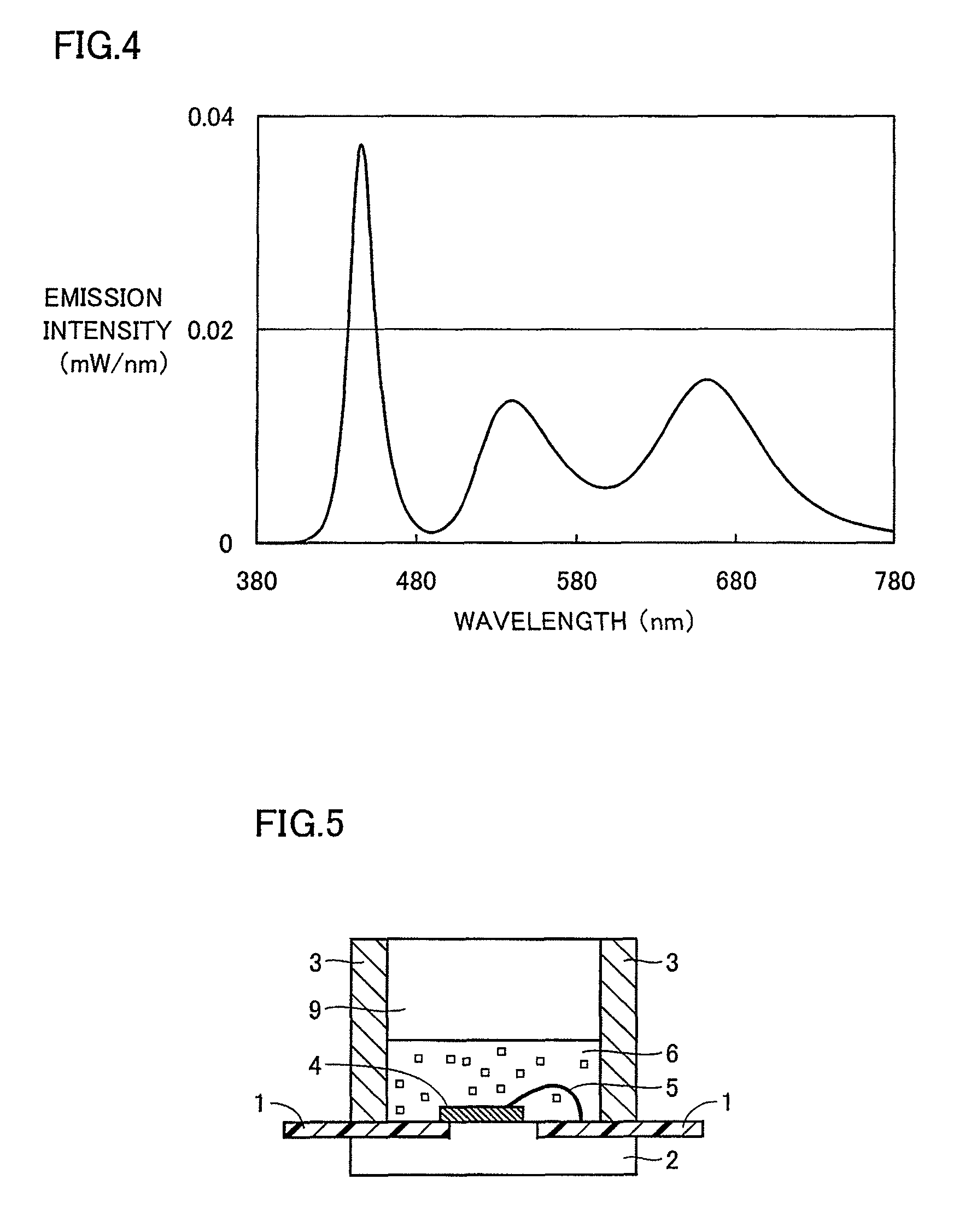
[0065]The present embodiment is identical to the light emitting apparatus of the first embodiment except that resin flakes 8 are contained in second wavelength conversion unit 7 of the first embodiment. FIG. 8 is a cross section of a light emitting apparatus in the third embodiment. Resin flakes 8 dispersively mixed in second wavelength conversion unit 7 are not particularly limited as long as they are an optically transparent material, and mainly a silicone or epoxy based material is used. While resin flakes 8 in the shape of beads are commonly used, the shape is not particularly limited to this. Respective sizes of resin flakes 8, however, are preferably uniform. In the present embodiment, flakes of a resin having a refractive index identical to or close to that of the resin layer forming second wavelength conversion unit 7 are used. Here, the refractive index of the resin flakes may be different from the refractive index of the resin layer so that light scattering is utilized. Fu...


PUM


Abstract

A light emitting apparatus includes a light emitting device emitting primary light and a wavelength conversion unit absorbing a part of the primary light to emit secondary light. The wavelength conversion unit includes a first wavelength conversion unit containing at least a nanocrystalline phosphor and a second wavelength conversion unit containing a rare-earth-activated phosphor or a transition-metal-element-activated phosphor. In the light emitting device, the first wavelength conversion unit and the second wavelength conversion unit are closely stacked in order.

Description

[0001]This nonprovisional application is based on Japanese Patent Application No. 2010-175873 filed on Aug. 5, 2010, No. 2010-230555 filed on Oct. 13, 2010, No. 2010-273091 filed on Dec. 8, 2010, No. 2011-045917 filed on Mar. 3, 2011, No. 2011-142412 filed on Jun. 28, 2011 and No. 2011-142413 filed on Jun. 28, 2011 with the Japan Patent Office, the entire contents of which are hereby incorporated by reference.BACKGROUND OF THE INVENTION[0002]1. Field of the Invention[0003]The present invention relates to a light emitting apparatus and a method for manufacturing the light emitting apparatus, and particularly to a light emitting apparatus using a phosphor excited by light emitted from a light source as well as a method for manufacturing the light emitting apparatus.[0004]2. Description of the Background Art[0005]As a next generation light emitting apparatus that is expected to consume less electrical power, have compact size, and exhibit high brightness, a light emitting apparatus usi...

Claims


Application Information

Patent Timeline
Patent Type & Authority Patents(United States)
IPC IPC(8): H01L51/00
CPCB82Y30/00C09K11/0883C09K11/70C09K11/7734C09K11/883H01L33/504H01L33/502H01L33/505H01L2224/48091H01L2224/48247H01L2924/1815H01L2924/00014C09K11/77348
Inventor ANNEN, KAZUNORIIZUMI, MAKOTOMIEDA, KIMIKOYOSHIMURA, KENICHIFUKUNAGA, HIROSHI
Owner SHARP KK
Why Eureka
Try Eureka