Method and system for an optical coupler for silicon photonics devices

a technology of silicon photonics and optical couplers, applied in the field of semiconductor processing, can solve the problems of cable bulk penalties, large power requirements, and complex structure, and achieve the effects of small improvement in reach, limited scalability, and limited scalability

Active Publication Date: 2015-02-05
CISCO TECH INC
View PDF6 Cites 68 Cited by
  • Summary
  • Abstract
  • Description
  • Claims
  • Application Information

AI Technical Summary

Problems solved by technology

They can be mitigated to some extent with equalization, coding, and shielding, but these techniques require considerable power, complexity, and cable bulk penalties while offering only modest improvements in reach and very limited scalability.

Method used


Image

  • Method and system for an optical coupler for silicon photonics devices
  • Method and system for an optical coupler for silicon photonics devices
  • Method and system for an optical coupler for silicon photonics devices

Examples


Embodiment Construction

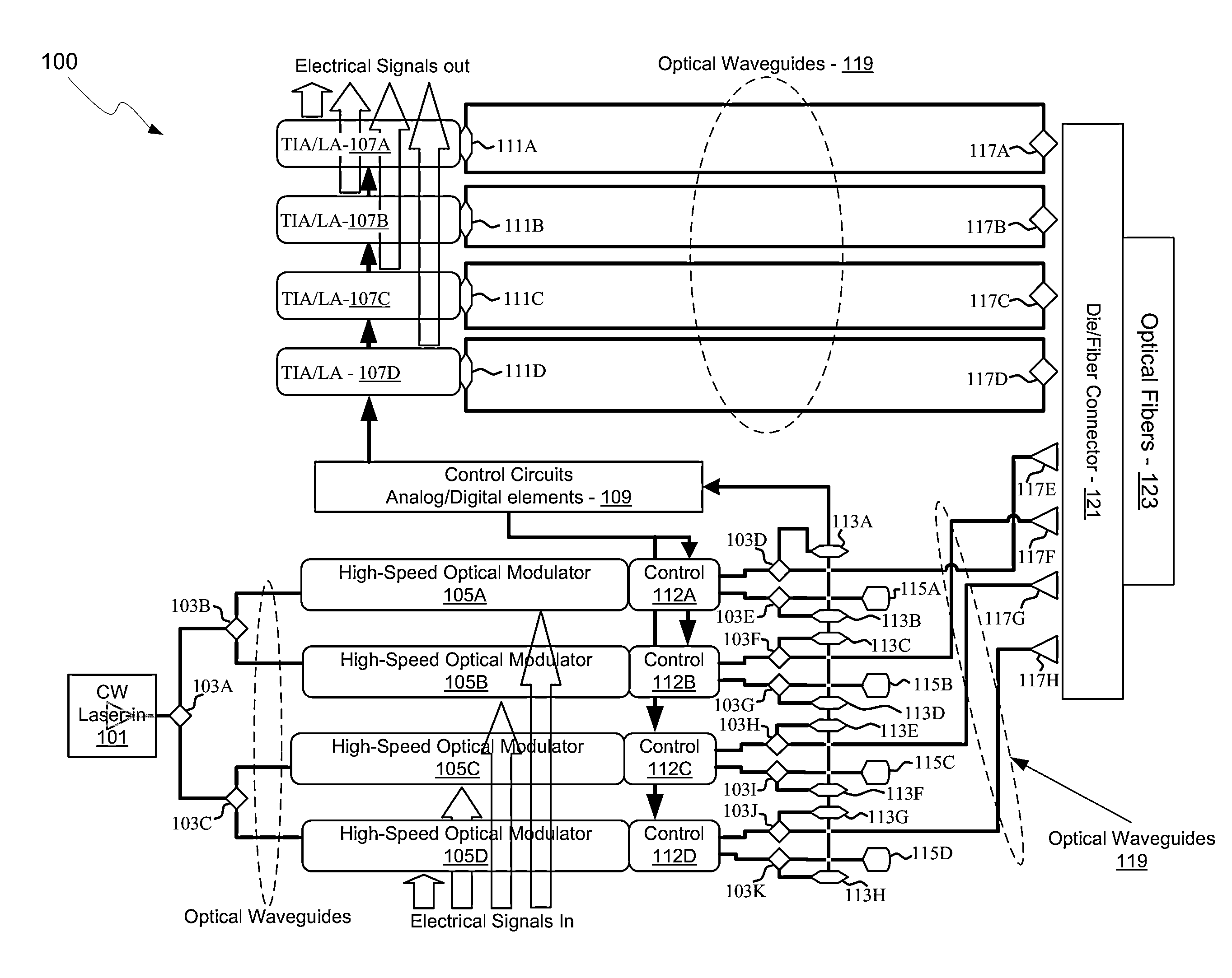
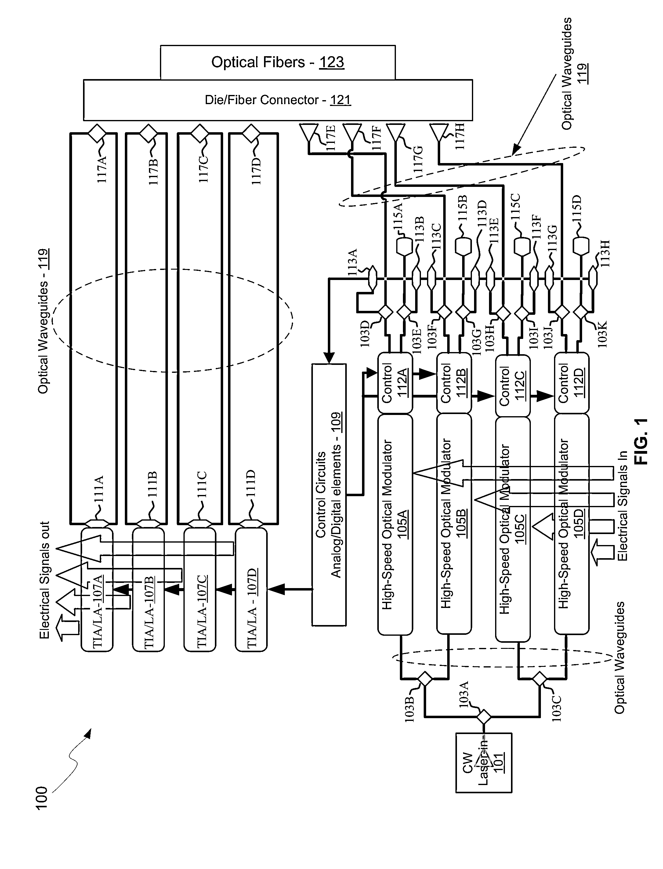
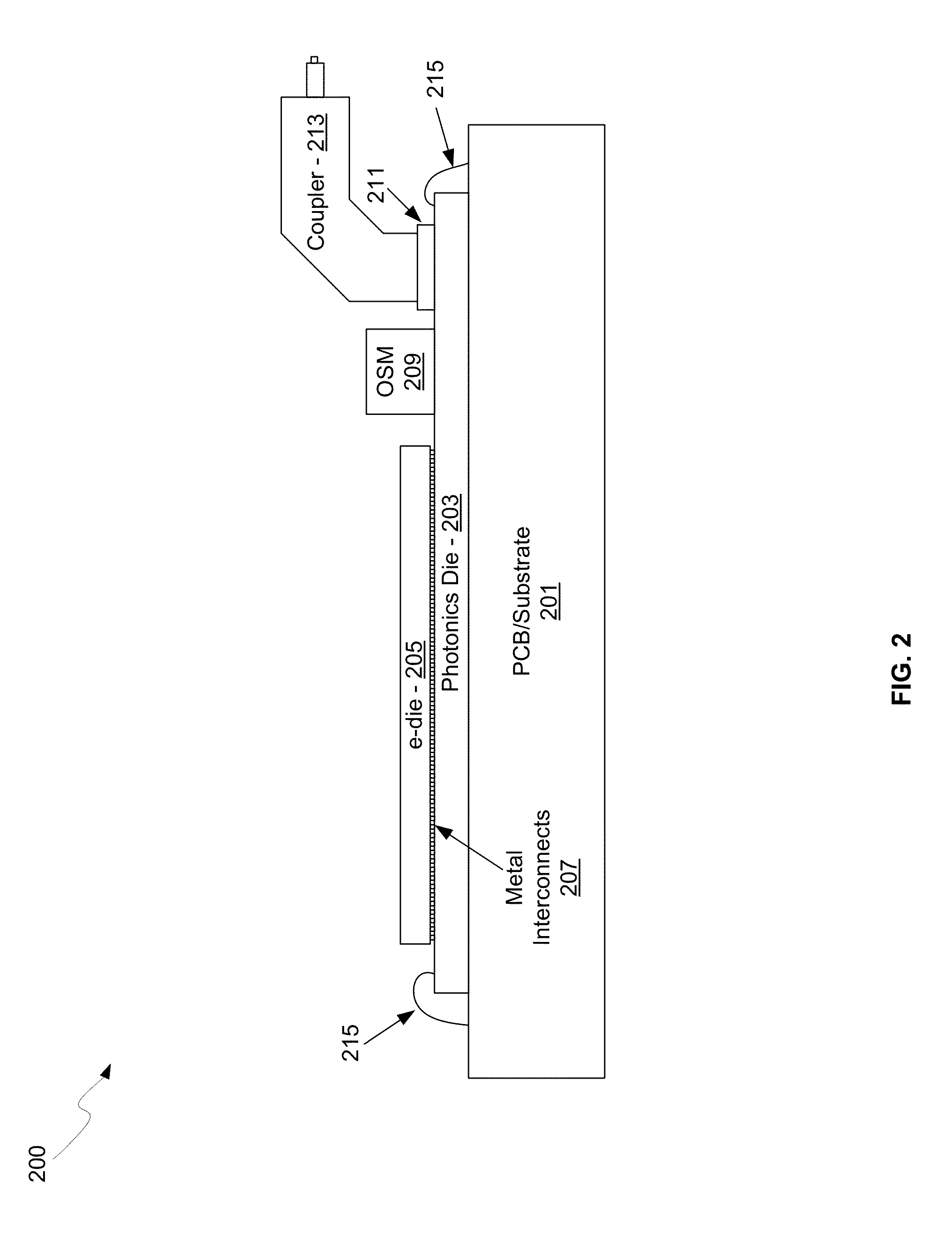
[0020]Certain aspects of the disclosure may be found in a method and system for an optical coupler for silicon photonics devices. Example aspects of the disclosure may comprise a photonics transceiver comprising a silicon photonics die, an electronics die, an optical source module, and a fiber connector, the fiber connector for receiving one or more optical fibers and comprising a die coupler and an optical coupling element. The die coupler may be bonded to a top surface of the photonics die and aligned above an array of grating couplers, where the optical coupling element may be removably attached to the die coupler and where the electronics die and the optical source module may be bonded to the top surface of the silicon photonics die. One or more continuous wave (CW) optical signals may be received in the silicon photonics die from the optical source module and the one or more received CW optical signals may be processed based on electrical signals received from the electronics d...


PUM


Abstract

Methods and systems for an optical coupler for photonics devices are disclosed and may include a photonics transceiver comprising a silicon photonics die, an optical source module, and a fiber connector for receiving optical fibers and including a die coupler and an optical coupling element. The die coupler may be bonded to a top surface of the photonics die and aligned above an array of grating couplers. The optical coupling element may be attached to the die coupler and the electronics die and the source module may be bonded to the top surface of the photonics die. A continuous wave (CW) optical signal may be received in the photonics die from the optical source module. Modulated optical signals may be received in the photonics die from optical fibers coupled to the fiber connector.

Description

CROSS-REFERENCE TO RELATED APPLICATIONS / INCORPORATION BY REFERENCE[0001]This application makes reference to, claims priority to, and claims the benefit of U.S. Provisional Application Ser. No. 61 / 958,666 filed on Aug. 2, 2013. This application also makes reference to U.S. Provisional Application 61 / 743,233 filed on Aug. 29, 2012.[0002]Each of the above cited references is hereby incorporated by reference in its entirety.FIELD[0003]Certain embodiments of the disclosure relate to semiconductor processing. More specifically, certain embodiments of the disclosure relate to a method and system for an optical coupler for silicon photonics devices.BACKGROUND[0004]As data networks scale to meet ever-increasing bandwidth requirements, the shortcomings of copper data channels are becoming apparent. Signal attenuation and crosstalk due to radiated electromagnetic energy are the main impediments encountered by designers of such systems. They can be mitigated to some extent with equalization, co...

Claims


Application Information

Patent Timeline
Patent Type & Authority Applications(United States)
IPC IPC(8): H04B10/40
CPCH04B10/40G02B6/428G02B6/4246G02B6/43G02B6/4214G02B6/4292
Inventor PETERSON, MARKWELCH, BRIANGLOECKNER, STEFFENDEDOBBELAERE, PETERMACK, MICHAEL
Owner CISCO TECH INC
Why Eureka
Try Eureka