Touch sensor and manufacturing method for the same, as well as transfer ribbon for touch sensor manufacturing

Inactive Publication Date: 2015-02-12
NISSHA PRINTING COMPANY
View PDF5 Cites 24 Cited by
  • Summary
  • Abstract
  • Description
  • Claims
  • Application Information

AI Technical Summary

Benefits of technology

The present invention provides a capacitance type touch sensor that has a simplified method of forming patterns. The sensor has a uniform insulation surface, ensuring proper insulation even when the electrodes are misaligned. Additionally, the sensor has integrated electrodes that do not have separate steps, which prevents poor conduction due to misalignment. These features improve the performance and quality of the touch sensor.

Problems solved by technology

Meanwhile, in forming an electrode or the like on a substrate, if an electrode film or the like is formed by repeating a sputtering method, a photolithography method, an etching method, or the like a plurality of times, the manufacturing cost is increased.

Method used


Image

  • Touch sensor and manufacturing method for the same, as well as transfer ribbon for touch sensor manufacturing
  • Touch sensor and manufacturing method for the same, as well as transfer ribbon for touch sensor manufacturing
  • Touch sensor and manufacturing method for the same, as well as transfer ribbon for touch sensor manufacturing

Examples


first embodiment

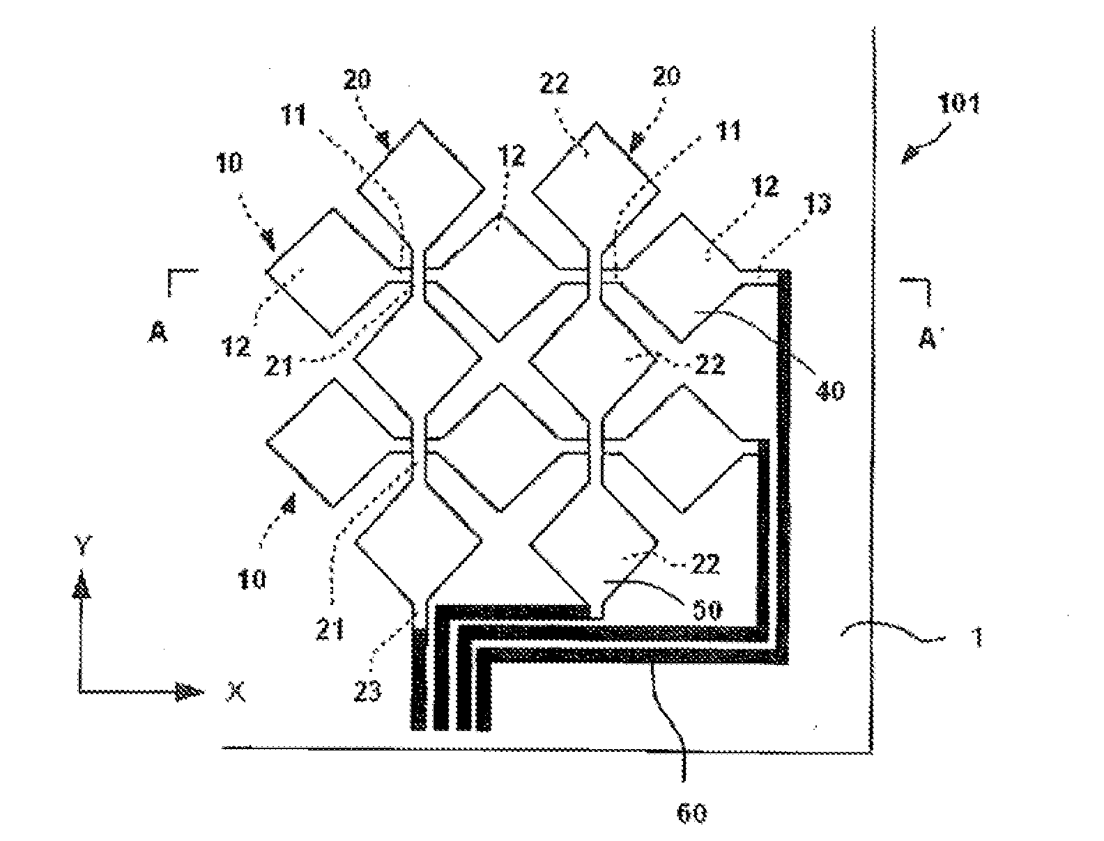
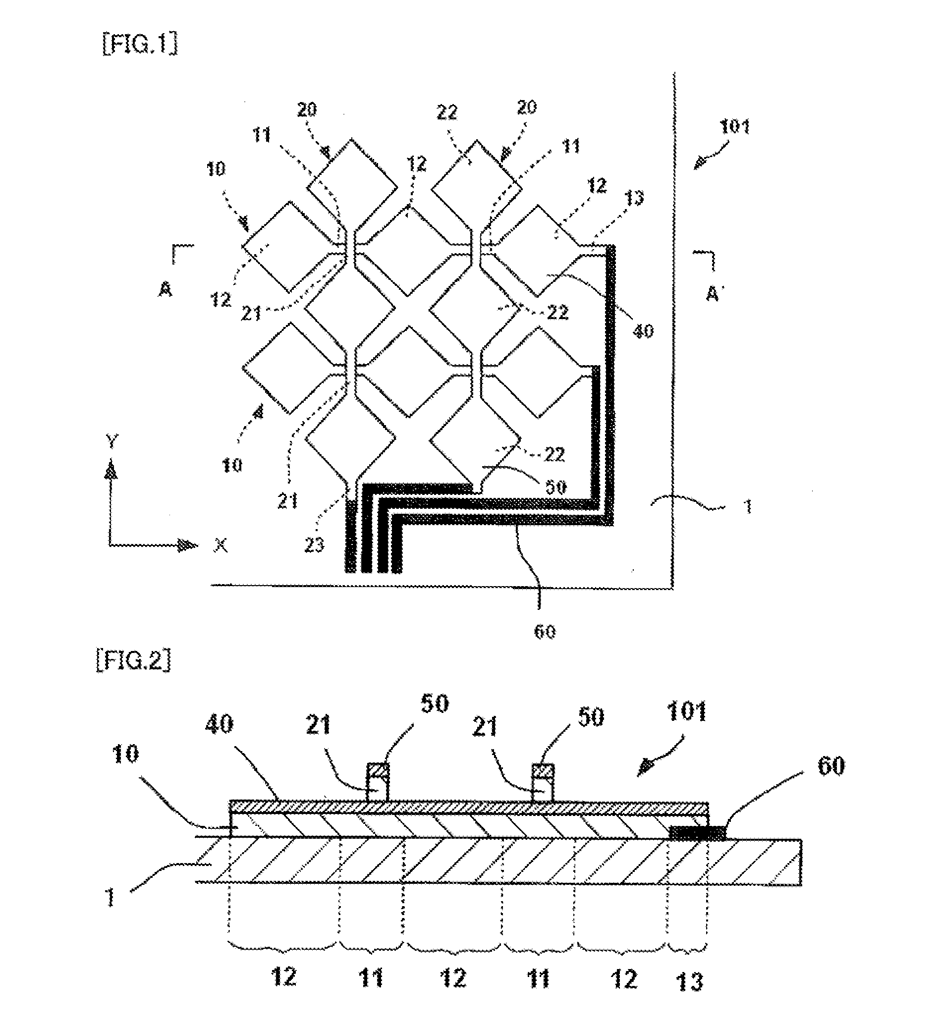
[0070]Hereinafter, an embodiment of a touch sensor according to the present invention will be described with reference to the drawings. FIG. 1 is a partially enlarged plan view showing an example of the touch sensor according to the present invention. FIG. 2 is an A-A′ cross-sectional view of FIG. 1.

[0071]A touch sensor 101 shown in FIG. 1 includes X electrode films 10 as a plurality of first electrode films and Y electrode films 20 as a plurality of second electrode films on one surface of one substrate.

[0072]The substrate 1 is an electrically insulating substrate and may be, for example, a glass substrate, a PET (polyethylene terephthalate) film, a PC (polycarbonate) film, a COP (cycloolefin polymer) film, a PVC (polyvinyl chloride) film, or the like. In particular, the COP film is preferred since it is excellent not only in optical isotropy but also in dimensional stability and further processing accuracy. It should be noted that when the substrate 1 is a glass substrate, the thi...

second embodiment

[0099]Next, a second embodiment will be described. It should be noted that the description of components common to those of the first embodiment is omitted and components only according to the second embodiment will be described.

[0100]Each routing wire 60 of the first embodiment is connected to the one end of the X electrode film 10 or the Y electrode film 20 from the substrate 1 side, but in the second embodiment, each routing wire 61 is configured to be connected to one end of the X electrode film 10 or the Y electrode film 20 from a side opposite to the substrate 1 (see FIG. 14).

[0101]In this case, in the manufacturing process for a touch sensor 102, first, a first transfer step (see FIGS. 15 to 17) and a second transfer step (see FIGS. 18 to 20) are conducted, and then a routing wire forming step (see FIG. 14) is conducted. In the routing wire forming step, the routing wires 61 are pattern-formed by screen printing or the like using a metal paste such as gold, silver, or copper....

third embodiment

[0103]Next, a third embodiment will be described. It should be noted that the description of components common to those of the first and second embodiments is omitted and components only according to the third embodiment will be described.

[0104]Each of the routing wires 60 and 61 of the first and second embodiments is connected to the one end of the X electrode film 10 or the Y electrode film 20 from the substrate 1 side or from the side opposite to the substrate 1, but in the third embodiment, each routing wire 62 is configured to extend from the X electrode film 10 or the Y electrode film 20 and be formed as a film integrated therewith. In other words, the material of the routing wires 62 is the same as that of the X electrode films 10 and the Y electrode films 20. In addition, the first insulating films 40 and the second insulating films 50 are formed on the routing wires 62 so as to cover the entireties thereof except for terminal portions thereof (see FIG. 21).

[0105]In this cas...


PUM


Abstract

A touch sensor including a plurality of first electrode films and a plurality of second electrode films which are formed on a surface of a substrate and are arranged in different directions from each other; and a manufacturing method for the same. The manufacturing method includes: a first transfer step, which uses a transfer ribbon made by at least an insulating layer and an electrode-imparting layer which are entirely sequentially stacked as a transfer layer upon an elongated release film, attaches to a substrate only a portion of the transfer layer to which heat and pressure have been applied, and by stripping the release film, transfers the transfer layer in at least the shape of a first electrode film; and a second transfer step including attaching only the portion of the transfer layer to which the heat and the pressure had been applied and stripping the release film.

Description

TECHNICAL FIELD[0001]The present invention relates to a capacitance type touch sensor having a plurality of first electrode films and a plurality of second electrode films which are formed on a surface of a substrate and are arranged in different directions from each other.BACKGROUND ART[0002]Conventionally, various touch sensors have been devised. For example, a capacitance type touch sensor (hereinafter, “touch sensor”) has been known, which includes a plurality of electrode films formed so as to intersect each other via an insulating layer and in which by moving a finger or the like close to a panel in which the electrode films are formed, a capacity is generated between, the electrode films of the panel, and a current that charges the generated capacity is detected, thereby performing position detection (see, e.g., Patent Document 1).[0003]A touch sensor 100 disclosed in Patent Document 1 includes a substrate 1, an input region 2, and routing wires 60. The input region 2 is a re...

Claims


Application Information

Patent Timeline
IPC IPC(8): H03K17/96B41M5/40B32B37/00
CPCH03K17/9622B32B37/025B41M5/40H03K2017/9613B41M2205/30H03K2217/960765B32B2307/202B32B2457/16B32B2457/208H03K2217/960755G06F2203/04103G06F3/0443G06F3/0446G06F3/0445
Inventor OKUMURA, SHUZOSAKASHITA, ASAKONAKAGAWA, EIJINAGASE, RYOHEIMATSUZAKI, TOMOHIRO
Owner NISSHA PRINTING COMPANY
Why Eureka
Try Eureka