Continuous whole-chip 3-dimensional dep cell sorter and related fabrication method

a technology of 3d microfluidic devices and sorters, which is applied in the direction of separation processes, instruments, laboratory glasswares, etc., can solve the problems of complex fluid routing and interfacing, the majority of multi-layer pdms devices demonstrated so far are not true 3d microfluidic devices, and the interlayer fluid communication is typically not effective,

Active Publication Date: 2015-02-12
RGT UNIV OF CALIFORNIA
View PDF3 Cites 9 Cited by
  • Summary
  • Abstract
  • Description
  • Claims
  • Application Information

AI Technical Summary

Benefits of technology

[0013]Embodiment 1: A 3-dimensional dielectrophoretic (DEP) sorting device, the device including: a first electrode; a second electrode; an electrically-insulating layer sandwiched between the first electrode and the second electrode, wherein: the electrically-insulating layer includes a separation passage with walls partially bounded by the first electrode and the second electrode, the electrically-insulating layer includes a collection passage smaller than the separation passage in cross-sectional thickness and located at an inter-electrode location between the first electrode and t

Problems solved by technology

Most multilayer PDMS devices demonstrated so far are not true 3D microfluidic devices.
Although multiple layers of 2D microfluidic networks can be stacked, there is typically no interlayer fluid communication due to the difficulty of fabricating high-resolution through-layer vias for fluidly connecting different layers in high yield.
Without through-layer vias, fluid routing and interfacing become complex issues for large scale 3D microfluidic networks.
Two-dimensional cell sorters typically have a maximum flow rate beyond which the cell sorting functionality is lost or s

Method used


Image

  • Continuous whole-chip 3-dimensional dep cell sorter and related fabrication method
  • Continuous whole-chip 3-dimensional dep cell sorter and related fabrication method
  • Continuous whole-chip 3-dimensional dep cell sorter and related fabrication method

Examples


Embodiment Construction

[0076]Examples of various implementations are illustrated in the accompanying drawings and described further below. It will be understood that the discussion herein is not intended to limit the claims to the specific implementations described. On the contrary, it is intended to cover alternatives, modifications, and equivalents as may be included within the spirit and scope of the invention as defined by the appended claims. In the following description, numerous implementation-specific details are set forth in order to provide a thorough understanding of the present invention. The present invention may be practiced without some or all of these implementation-specific details. In other instances, well-known process operations have not been described in detail in order not to unnecessarily obscure the present invention.

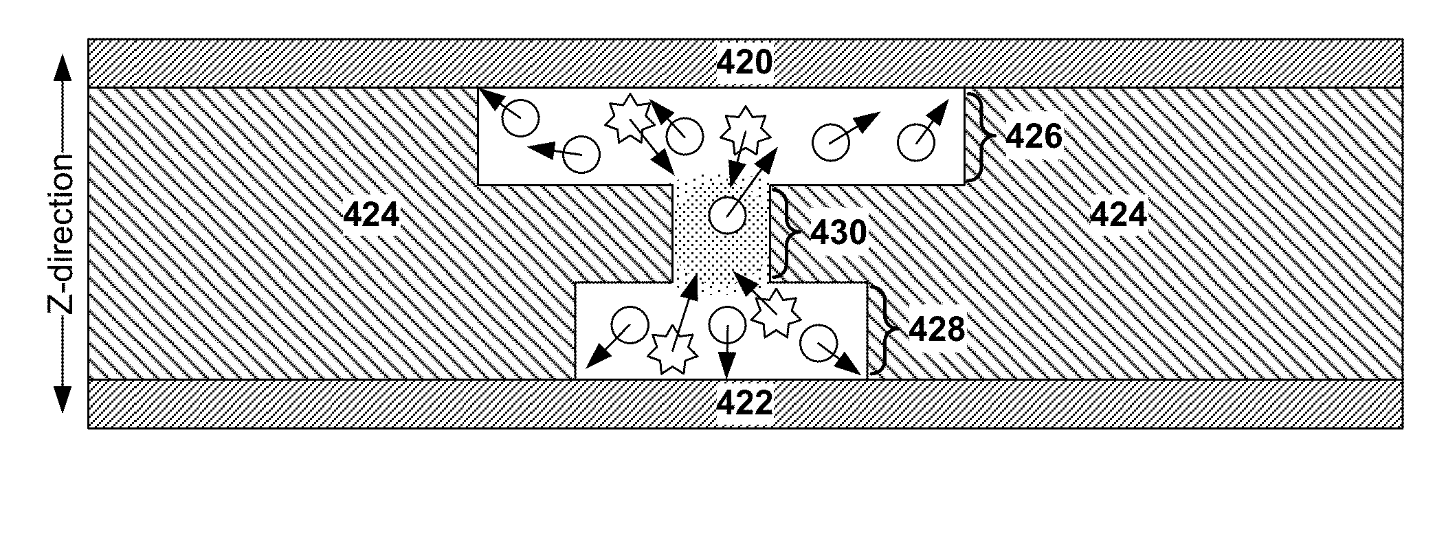
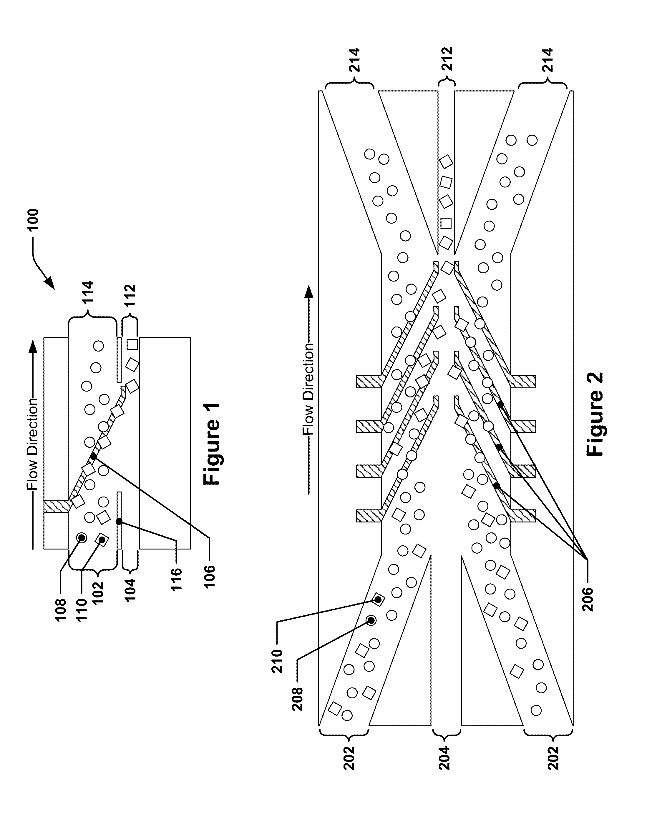
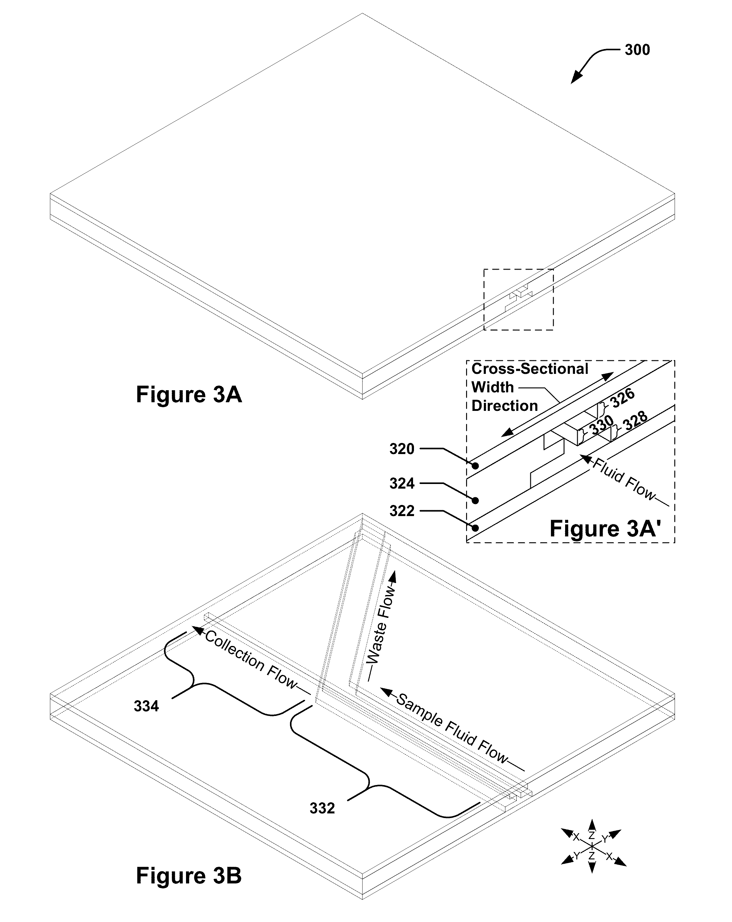
[0077]It is to be understood that while the discussion below may focus primarily on structures or devices such as cell sorters for sorting biological materials, e.g., ...


PUM


Abstract

A 3-dimensional PDMS cell sorter having multiple passages in a PDMS layer that follow the same path in a DEP separation region and that are in fluid communication with each other within that region. The passages may differ in width transverse to the flow direction within the passages. Flat plates may sandwich the PDMS layer; each plate may have a planar electrode used to generate a DEP field within a sample fluid flowed within the passages. The DEP field may concentrate target cells or particulates within one of the passages within the DEP separation region. The passages may diverge after the DEP-separation region, leaving one passage with a high concentration of target cells or particulates. Techniques for manufacturing such structures, as well as other micro-fluidic structures, are also provided.

Description

CROSS REFERENCE TO RELATED APPLICATIONS[0001]This application claims benefit under 35 U.S.C. §371 to PCT / US13 / 34145 filed on Mar. 27, 2013, and under 35 U.S.C. §119(e) to U.S. Provisional Application No. 61 / 616,385, filed Mar. 27, 2012, titled “CONTINUOUS WHOLE-CHIP 3-DIMENSIONAL DEP CELL SORTER AND ITS FABRICATION”, and U.S. Provisional Application No. 61 / 799,451, filed Mar. 15, 2013, titled “CONTINUOUS WHOLE-CHIP 3-DIMENSIONAL DEP CELL SORTER AND RELATED FABRICATION METHOD,” both of which are hereby incorporated by reference herein in their entirety.GOVERNMENT LICENSE RIGHTS[0002]This invention was made with US Government support under Grant No. 0901154, awarded by the National Science Foundation. The US Government has certain rights in this invention.BACKGROUND OF THE INVENTION[0003]Microfluidic devices present a cost-effective mechanism for performing small-scale fluidic manipulation on various fluid-entrained samples. For example, some microfluidic devices may be used to route,...

Claims


Application Information

Patent Timeline
IPC IPC(8): B03C5/00
CPCB03C5/005B01L3/502761B01L2200/0652B01L2300/0816B01L2300/0864B01L2300/0867B01L2400/0424B01L2400/0655B03C5/026B03C2201/26G01N15/0656G01N27/44778G01N2015/0065G01N2015/1081
Inventor CHIOU, PEI-YU E.HUANG, KUO-WEIFAN, YU-JUIKUNG, YU-CHUN
Owner RGT UNIV OF CALIFORNIA
Why Eureka
Try Eureka