Electronic module and method of manufacturing the same

a technology of electronic modules and mold compounds, applied in the direction of electrical apparatus contruction details, printed circuit non-printed electric components association, semiconductor/solid-state device details, etc., can solve the problems of high and rapid heat generation, dissipation of generated heat, and damage to the function of batteries and motors, so as to increase the contact surface or interface, and reduce the probability of delamination. , the effect of reducing the probability of delamination

Inactive Publication Date: 2015-02-12
INFINEON TECH AG
View PDF7 Cites 1 Cited by
  • Summary
  • Abstract
  • Description
  • Claims
  • Application Information

AI Technical Summary

Benefits of technology

[0016]By providing a spacing element having a lateral surface comprising surface structures it may be possible to increase a contacting surface or interface between the spacing element and the mold compound. By increasing the contacting surface or interface between the spacing element and the mold compound it may be possible to decrease the probability of delamination.
[0017]In particular, delamination of the mold compound and / or between the electronic chip and the spacing element and / or the mold compound may be reduced. Such a delamination may particularly occur due to different thermal expansion of the mold compound and of the electronic chip and / or the material of the spacing element and may lead to the failure of the electronic module, e.g. due to breaking of electrical paths from and to the electronic component. However, since the surface structures may increase the total surface being available for direct contacting between the mold compound and the spacing element the failure risk of the electronic module may be decreased. In particular, an improved electronic module may be provided which may fulfil its functions for more temperature cycles, i.e. heating up and cooling down again, without breaking of electronics or electric paths in the electronic module due to delamination effects, for example.

Problems solved by technology

These batteries and electro motors are typically heavily strained or stressed in operation during the charging and discharging processes leading to a high and rapid heat generation which may be destructive for the function of the batteries and motors.
Thus, the dissipation of the generated heat is an important issue to be taken into consideration when constructing or designing such power modules.

Method used


Image

  • Electronic module and method of manufacturing the same
  • Electronic module and method of manufacturing the same
  • Electronic module and method of manufacturing the same

Examples


Embodiment Construction

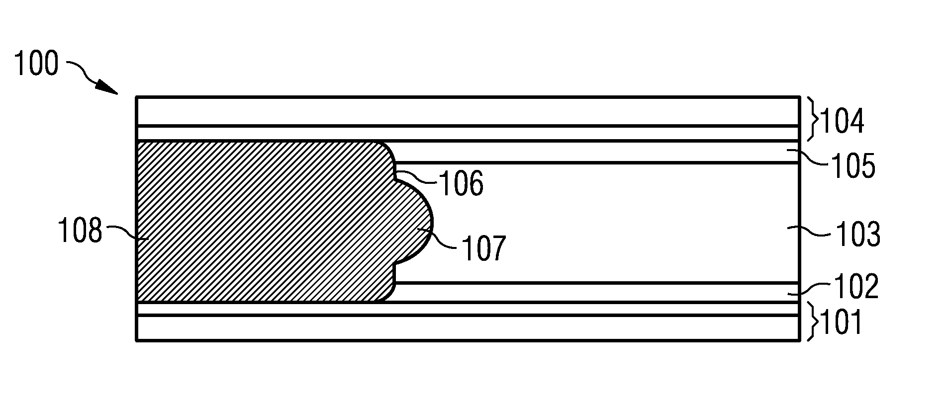
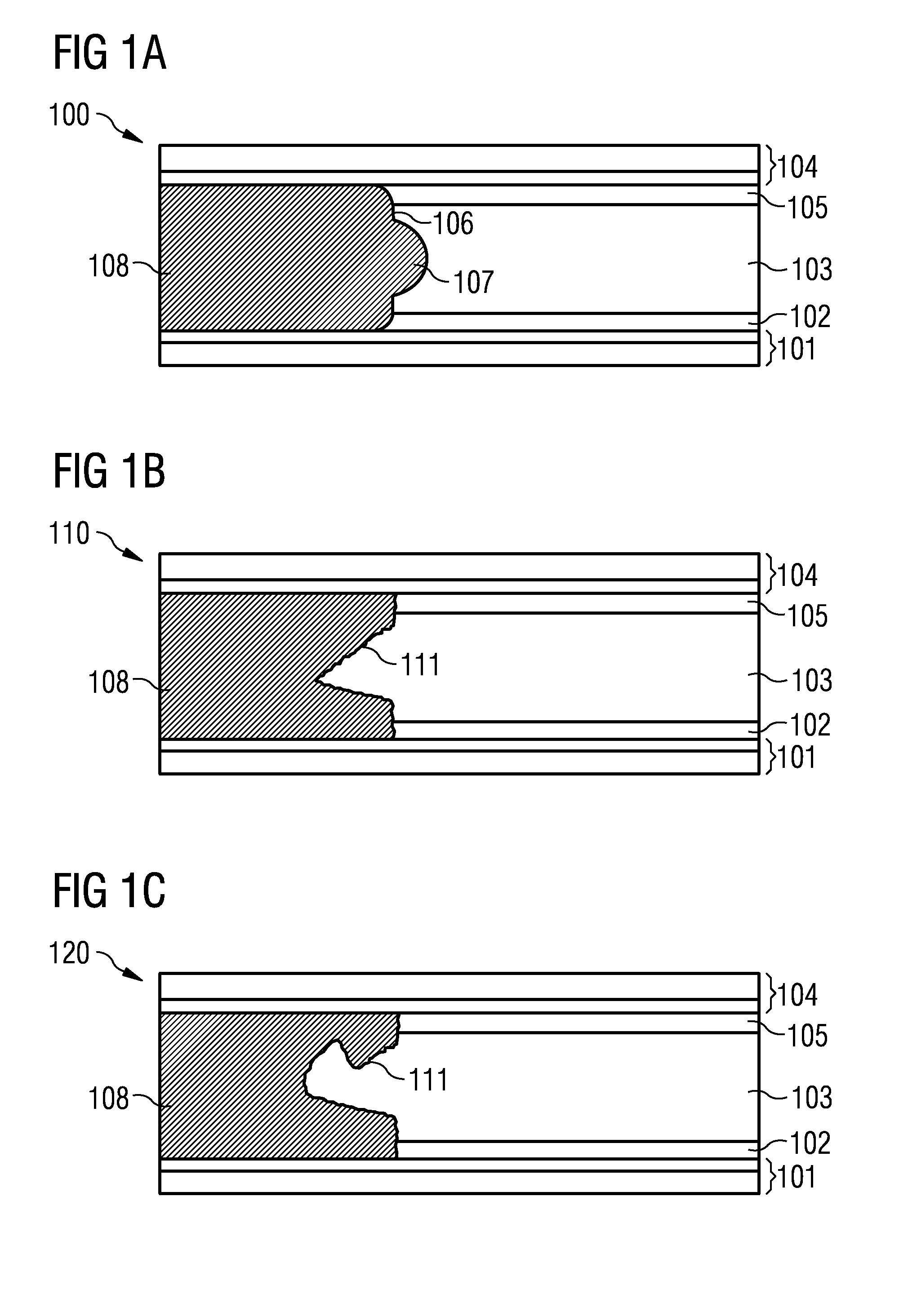
[0023]In the following, further exemplary embodiments of the electronic module and the method of manufacturing the same will be explained. It should be noted that embodiments described in the context of the electronic module may also be combined with embodiments of the method of manufacturing the electronic module and vice versa.

[0024]In particular, the spacing element comprises a conductive material. For example, the conductive material may be thermally and / or electrically conductive. The spacing element may also fulfil a levelling effect balancing differences in height of components or layers of the electronic module. In particular, the electronic chip may comprise or may be formed by a power transistor, i.e. a switching element suitable for switching electrical power in the amount of several tens or hundreds of watts. Such power transistors have to be distinguished from transistors used for switching information signals, e.g. in integrated circuits of a processor or memory. Alter...


PUM

PropertyMeasurementUnit
thicknessaaaaaaaaaa
thicknessaaaaaaaaaa
thicknessaaaaaaaaaa

Abstract

According to an exemplary aspect an electronic module is provided, wherein the electronic module comprises an electronic chip comprising at least one electronic component, a spacing element comprising a main surface arranged on the electronic chip and being in thermally conductive connection with the at least one electronic component, and a mold compound at least partially enclosing the electronic chip and the spacing element, wherein the spacing element comprises a lateral surface which is in contact to the mould compound and comprises surface structures.

Description

BACKGROUND OF THE INVENTION[0001]1. Field of the Invention[0002]The present invention relates to an electronic module. Moreover, the present invention relates to a method of manufacturing an electronic module.[0003]2. Description of the Related Art[0004]In the art a plurality of electronic modules are known which comprises an electronic or semiconductor chip providing some electronic functionality. The electronic chip may be arranged or placed on a substrate and may be housed or packaged by a mold compound enclosing the electronic chip.[0005]In particular, due to the housing by the mold compound the dissipation of heat generated by the electronic chip may be an object. This is particularly true in case the electronic module forms or is part of a power module, i.e. a module adapted and intended to handle a rather high power, e.g. several orders of magnitudes higher than for electronic modules used in the field of information technology.[0006]Such power modules are used in batteries o...

Claims


Application Information

Patent Timeline
Patent Type & Authority Applications(United States)
IPC IPC(8): H05K1/18
CPCH05K1/185H05K3/4608H01L2924/13055Y10T29/49002H01L2924/00H01L21/4871H01L21/565H01L23/3121H01L23/4334H01L24/32H01L24/83H01L2224/32225H01L2224/32245H01L2224/838H01L2224/83801H01L2224/8384
Inventor WINTER, FRANKGEITNER, OTTMARNIKITIN, IVANHOEGERL, JUERGEN
Owner INFINEON TECH AG
Why Eureka
Try Eureka