

PCB backdrilling method and system
- Summary
- Abstract
- Description
- Claims
- Application Information
AI Technical Summary
Benefits of technology
Problems solved by technology
Method used
Image

Examples
embodiment 1
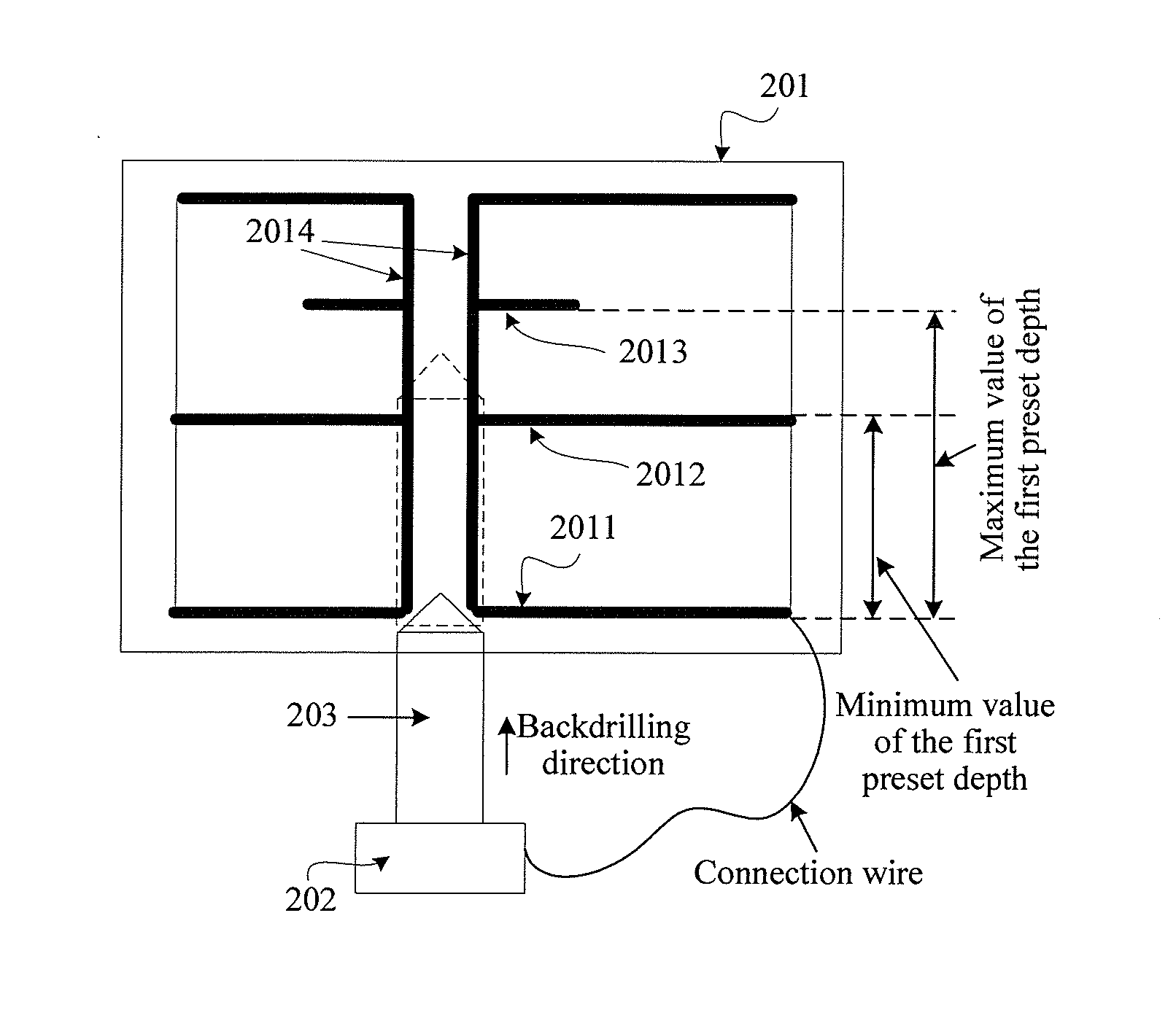
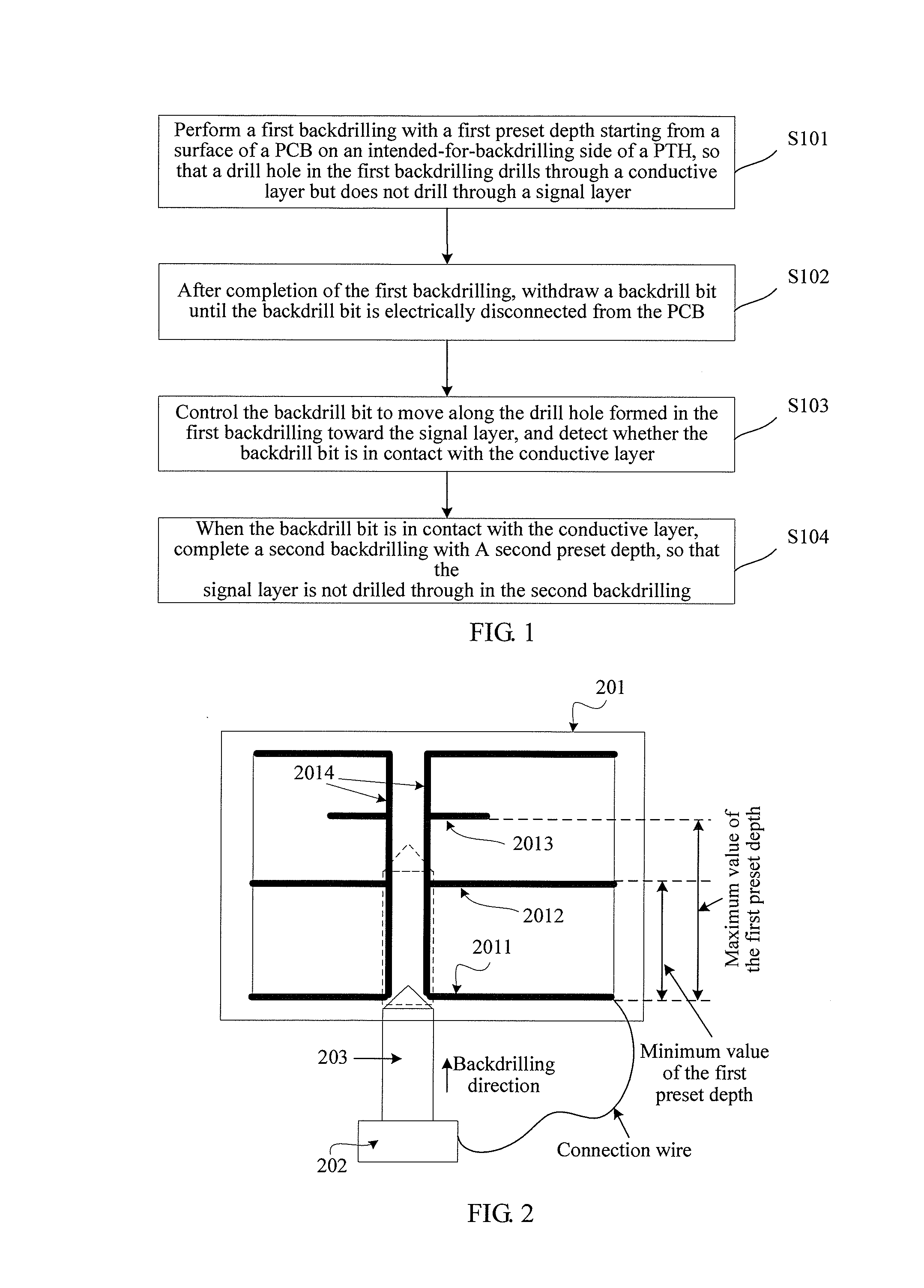
[0035]Refer to FIG. 1, which is a schematic method flowchart of a PCB backdrilling method according to the present invention, where a conductive layer is disposed between a surface of a printed circuit board PCB on an intended-for-backdrilling side of a plated through hole PTH and a target signal layer of the PCB, the conductive layer is connected to the PTH, and the target signal layer is a signal layer corresponding to a current backdrilling task, and the method includes the following steps:
[0036]Here it should be noted that the PTH of the PCB is a plated through hole on the PCB. Generally, the PTH is connected to at least upper and lower surface copper foils of the PCB and the target signal layer in the PCB. When backdrilling is performed, the backdrilling begins with a PCB side of the PTH. That is, the drilling is from a copper foil on that side to the target signal layer. The target signal layer is emphasized here primarily because the PCB includes multiple signal layers, and, ...
embodiment 2
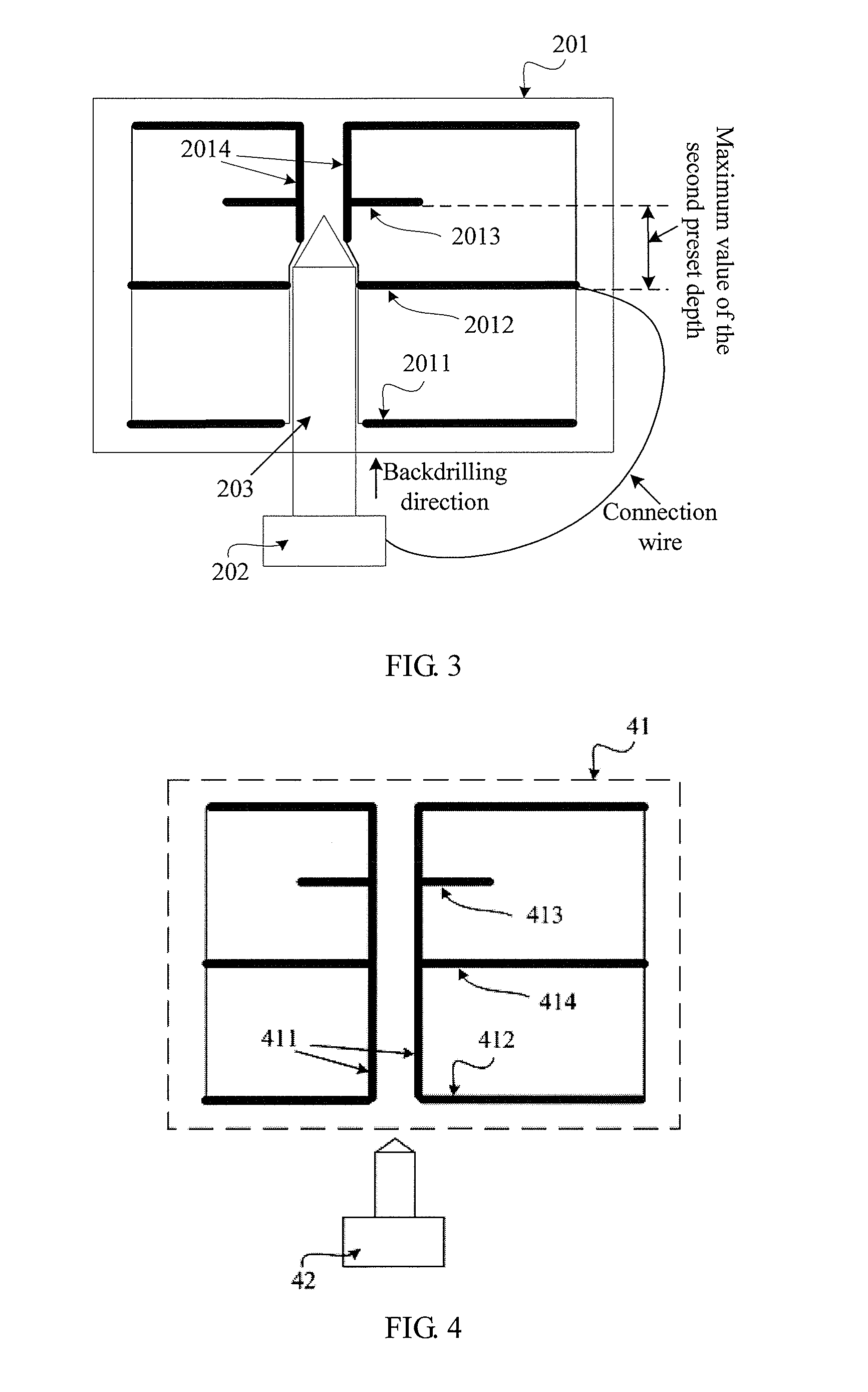
[0066]Corresponding to the foregoing one PCB backdrilling method, this embodiment of the present invention further provides a PCB backdrilling system. Refer to FIG. 4, which is a schematic diagram of a system structure of a PCB backdrilling system according to the present invention, where a conductive layer is disposed between a surface of a PCB on an intended-for-backdrilling side of a PTH and a target signal layer of the PCB, the conductive layer is connected to the PTH, and the target signal layer is a signal layer corresponding to a current backdrilling task, and the system includes the PCB 41 and a backdrilling device 42. The following further describes an internal structure and a connection relationship of the system with reference to working principles of the system.
[0067]The PCB 41 includes the PTH 411, the surface 412 of the PCB on the intended-for-backdrilling side of the PTH, the target signal layer 413, and the conductive layer 414.
[0068]The surface 412 of the PCB on the...
PUM
| Property | Measurement | Unit |
|---|---|---|
| Thickness | aaaaa | aaaaa |
| Electrical conductor | aaaaa | aaaaa |
Abstract
Description
Claims
Application Information